JAJSF83E June 2013 – February 2020 LMZ31707
PRODUCTION DATA.
- 1 特長
- 2 アプリケーション
- 3 概要
- 4 改訂履歴
- 5 Specifications
- 6 Device Information
- 7 Typical Characteristics (PVIN = VIN = 12 V)
- 8 Typical Characteristics (PVIN = VIN = 5 V)
- 9 Typical Characteristics (PVIN = 3.3 V, VIN = 5 V)
-
10Application Information
- 10.1 Adjusting the Output Voltage
- 10.2 Capacitor Recommendations for the LMZ31707 Power Supply
- 10.3 Transient Response
- 10.4 Transient Waveforms
- 10.5 Application Schematics
- 10.6 Custom Design With WEBENCH® Tools
- 10.7 VIN and PVIN Input Voltage
- 10.8 3.3 V PVIN Operation
- 10.9 Power Good (PWRGD)
- 10.10 SYNC_OUT
- 10.11 Parallel Operation
- 10.12 Light Load Efficiency (LLE)
- 10.13 Power-Up Characteristics
- 10.14 Pre-Biased Start-up
- 10.15 Remote Sense
- 10.16 Thermal Shutdown
- 10.17 Output On/Off Inhibit (INH)
- 10.18 Slow Start (SS/TR)
- 10.19 Overcurrent Protection
- 10.20 Synchronization (CLK)
- 10.21 Sequencing (SS/TR)
- 10.22 Programmable Undervoltage Lockout (UVLO)
- 10.23 Layout Considerations
- 10.24 EMI
- 11デバイスおよびドキュメントのサポート
- 12メカニカル、パッケージ、および注文情報
10.18 Slow Start (SS/TR)
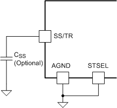
Connecting the STSEL pin to AGND and leaving SS/TR pin open enables the internal SS capacitor with a slow-start interval of approximately 1.2 ms. Adding additional capacitance between the SS pin and AGND increases the slow-start time. Increasing the slow-start time reduces inrush current seen by the input source and reduce the current seen by the device when charging the output capacitors. To avoid the activation of current limit and ensure proper start-up, the SS capacitor can need to be increased when operating near the maximum output capacitance limit.
Figure 29 shows an additional SS capacitor connected to the SS/TR pin and the STSEL pin connected to AGND. See Table 6 for SS capacitor values and timing interval.
 Figure 29. Slow-Start Capacitor (CSS) and STSEL Connection
 Table 6. Slow-Start Capacitor Values and Slow-Start Time
| CSS (nF) | OPEN | 3.3 | 4.7 | 10 | 15 | 22 | 33 |
|---|---|---|---|---|---|---|---|
| SS Time (msec) | 1.2 | 2.1 | 2.5 | 3.8 | 5.1 | 7.0 | 9.8 |