JAJSBA0Q January 2000 – December 2017 LP2950-N , LP2951-N
PRODUCTION DATA.
- 1 特長
- 2 アプリケーション
- 3 概要
- 4 改訂履歴
- 5 Voltage Options
- 6 Pin Configuration and Functions
- 7 Specifications
-
8 Detailed Description
- 8.1 Overview
- 8.2 Functional Block Diagrams
- 8.3 Feature Description
- 8.4 Device Functional Modes
-
9 Application and Implementation
- 9.1 Application Information
- 9.2
Typical Applications
- 9.2.1 1-A Regulator with 1.2-V Dropout
- 9.2.2 300-mA Regulator with 0.75-V Dropout
- 9.2.3 Wide Input Voltage Range Current Limiter
- 9.2.4 Low Drift Current Source
- 9.2.5 5-V Current Limiter
- 9.2.6 Regulator with Early Warning and Auxiliary Output
- 9.2.7 Latch Off When Error Flag Occurs
- 9.2.8 2-A Low Dropout Regulator
- 9.2.9 5-V Regulator with 2.5-V Sleep Function
- 9.2.10 Open Circuit Detector for 4 → 20-mA Current Loop
- 9.2.11 Regulator with State-of-Charge Indicator
- 9.2.12 Low Battery Disconnect
- 9.2.13 System Overtemperature Protection Circuit
- 10Power Supply Recommendations
- 11Layout
- 12デバイスおよびドキュメントのサポート
- 13メカニカル、パッケージ、および注文情報
パッケージ・オプション
メカニカル・データ(パッケージ|ピン)
サーマルパッド・メカニカル・データ
発注情報
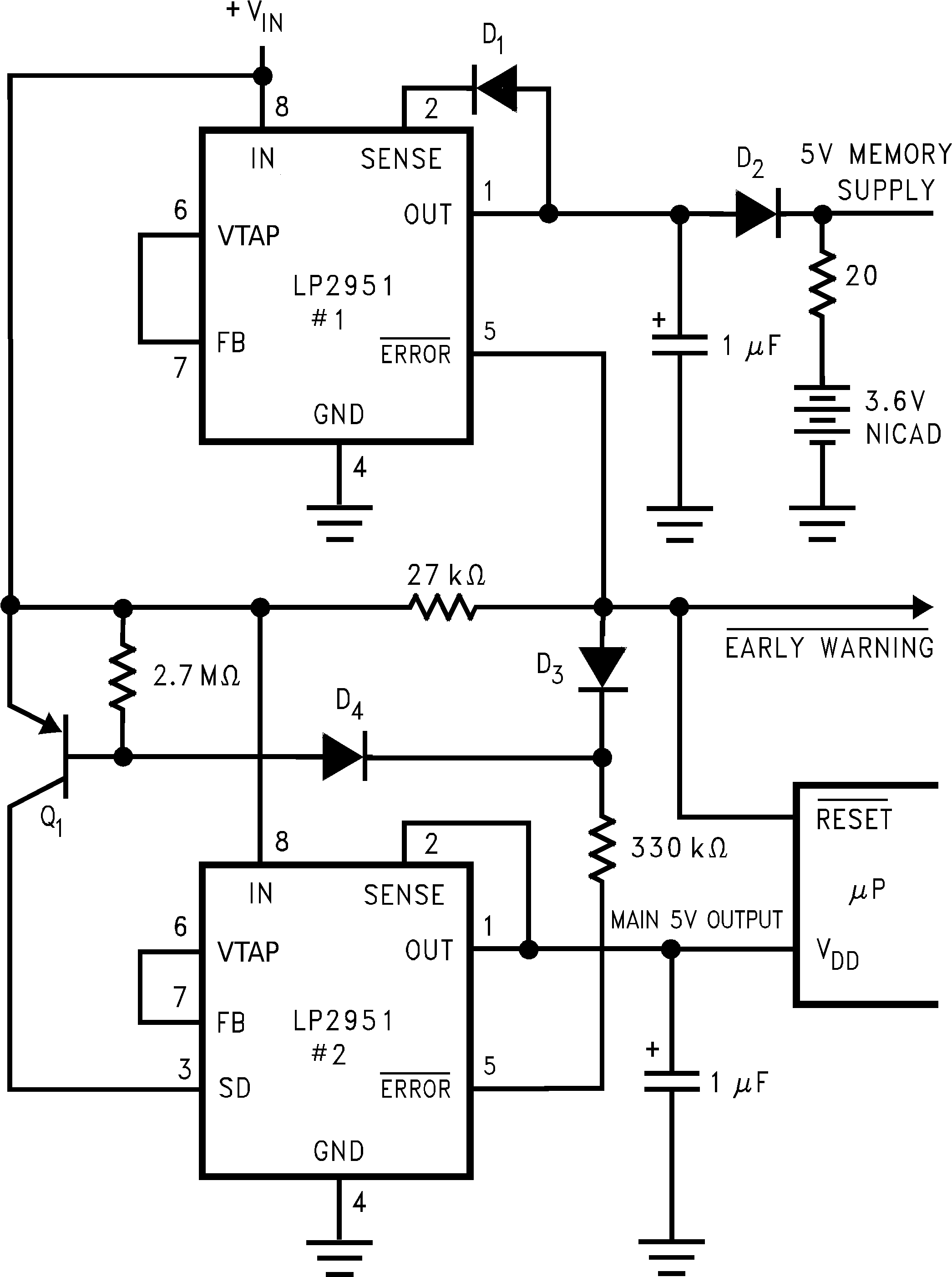
9.2.6 Regulator with Early Warning and Auxiliary Output
The LP2951 can be used to build a Regulator with early warning and auxiliary output as Figure 48 shows. it has below features:
- Early warning flag on low input voltage
- Main output latches off at lower input voltages
- Battery backup on auxiliary output
- Operation: VOUT of regulator 1 is programmed one diode drop above 5 V. Its error flag becomes active when VIN ≤ 5.7 V. When VIN drops below 5.3 V, the error flag of regulator 2 becomes active and via Q1 latches the main output off. When VIN again exceeds 5.7 V regulator 1 is back in regulation and the early warning signal rises, unlatching regulator 2 via D3.
 Figure 48. Regulator With Early Warning and Auxiliary Output