SNVS323I December 2004 – February 2016 LP38690-ADJ , LP38692-ADJ
PRODUCTION DATA.
- 1 Features
- 2 Applications
- 3 Description
- 4 Revision History
- 5 Pin Configuration and Functions
- 6 Specifications
- 7 Detailed Description
-
8 Application and Implementation
- 8.1 Application Information
- 8.2 Typical Application
- 9 Power Supply Recommendations
- 10Layout
- 11Device and Documentation Support
- 12Mechanical, Packaging, and Orderable Information
パッケージ・オプション
メカニカル・データ(パッケージ|ピン)
サーマルパッド・メカニカル・データ
発注情報
10 Layout
10.1 Layout Guidelines
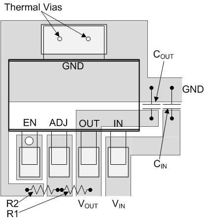
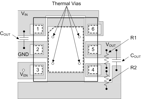
Good PC layout practices must be used or instability can be induced because of ground loops and voltage drops. The input and output capacitors must be directly connected to the IN, OUT, and GND pins of the regulator using traces which do not have other currents flowing in them (Kelvin connect).
The best way to do this is to lay out CIN and COUT near the device with short traces to the IN, OUT, and GND pins. The regulator ground pin must be connected to the external circuit ground so that the regulator and its capacitors have a single point ground.
Stability problems have been seen in applications where vias to an internal ground plane were used at the ground points of the device and the input and output capacitors. This was caused by varying ground potentials at these nodes resulting from current flowing through the ground plane. Using a single point ground technique for the regulator and the regulator capacitors fix the problem. Because high current flows through the traces going into IN and coming from OUT, Kelvin connect the capacitor leads to these pins so there is no voltage drop in series with the input and output capacitors.
10.2 Layout Examples
 Figure 33. LP38692-ADJ SOT-223 Package
 Figure 34. LP3869x-ADJ WSON Package
10.3 WSON Mounting
The NGG0006A (No Pullback) 6-lead WSON package requires specific mounting techniques which are detailed in AN-1187 Leadless Leadframe Package (LLP), SNOA401. The pad style which to use with the WSON package is the NSMD (non-solder mask defined) type. Additionally, TI recommends the PCB terminal pads to be 0.2 mm longer than the package pads to create a solder fillet to improve reliability and inspection.
The input current is split between two IN pins, 1 and 6. The two IN pins must be connected together to ensure that the device can meet all specifications at the rated current.
The thermal dissipation of the WSON package is directly related to the printed circuit board construction and the amount of additional copper area connected to the DAP.
The DAP (exposed pad) on the bottom of the WSON package is connected to the die substrate with a conductive die attach adhesive. The DAP has no direct electrical (wire) connection to any of the pins. There is a parasitic PN junction between the die substrate and the device ground. As such, it is strongly recommend that the DAP be connected directly to the ground at device lead 2 (that is, GND). Alternately, but not recommended, the DAP may be left floating (that is, no electrical connection). The DAP must not be connected to any potential other than ground.