SNVS323I December 2004 – February 2016 LP38690-ADJ , LP38692-ADJ
PRODUCTION DATA.
- 1 Features
- 2 Applications
- 3 Description
- 4 Revision History
- 5 Pin Configuration and Functions
- 6 Specifications
- 7 Detailed Description
-
8 Application and Implementation
- 8.1 Application Information
- 8.2 Typical Application
- 9 Power Supply Recommendations
- 10Layout
- 11Device and Documentation Support
- 12Mechanical, Packaging, and Orderable Information
パッケージ・オプション
メカニカル・データ(パッケージ|ピン)
サーマルパッド・メカニカル・データ
発注情報
5 Pin Configuration and Functions
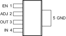
NDC Package (LP38692-ADJ only)
5-Pin SOT-223
Top View

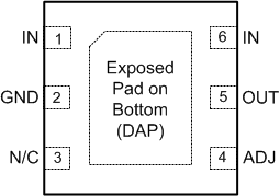
NGG Package (LP38690-ADJ)
6-Pin WSON
Top View

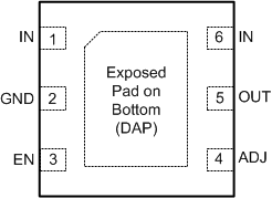
NGG Package (LP38692-ADJ)
6-Pin WSON
Top View

Pin Functions
| PIN | I/O | DESCRIPTION | |||
|---|---|---|---|---|---|
| LP38690-ADJ | LP38692-ADJ | ||||
| NAME | WSON | WSON | SOT-223 | ||
| ADJ | 4 | 4 | 2 | O | The ADJ pin is used to set the regulated output voltage by connecting it to the external resistors R1 and R2 (see Simplified Schematic LP38690-ADJ and Simplified Schematic LP38692-ADJ). |
| DAP | √ | √ | — | — | WSON only - The DAP (exposed pad) functions as a thermal connection when soldered to a copper plane. See Layout Guidelines for more information. |
| EN(1) | — | 3 | 1 | I | The EN pin allows the part to be turned to an ON or OFF state by pulling this pin high or low. |
| GND | 2 | 2 | 5 | — | Circuit ground for the regulator. For the SOT-223 package this is thermally connected to the die and functions as a heat sink when the soldered down to a large copper plane. |
| IN | 1, 6 | 1, 6 | 4 | I | This is the input supply voltage to the regulator. For WSON devices, both IN pins must be tied together for full current operation (250 mA maximum per pin). |
| NC(2) | 3 | — | — | — | No internal connection. |
| OUT | 5 | 5 | 3 | I | Regulated output voltage. |
(1) The EN pin is only available on the LP38692-ADJ.
(2) Pin 3 on the LP38690-ADJ is not used.