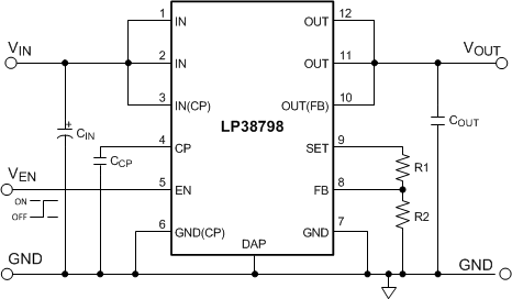
The LP38798-ADJ is a high-performance, low-noise LDO that can supply up to 800 mA output current. Designed to meet the requirements of sensitive RF/Analog circuitry, the LP38798-ADJ implements a novel linear topology on an advanced CMOS process to deliver ultra-low output noise and high PSRR at switching power supply frequencies. The LP38798SD-ADJ is stable with both ceramic and tantalum output capacitors and requires a minimum output capacitance of only 1 µF for stability.
The LP38798-ADJ can operate over a wide input voltage range (3 V to 20 V) making it well suited for many post-regulation applications.
PART NUMBER | PACKAGE | BODY SIZE (NOM) |
---|---|---|
LP38798 | WSON (12) | 4.00 mm × 4.00 mm |
space
space
space
space
space
space
Changes from E Revision (August 2016) to F Revision
Changes from D Revision (June 2016) to E Revision
Changes from C Revision (June2016) to D Revision
Changes from B Revision (December 2014) to C Revision
Changes from A Revision (May 2013) to B Revision
PIN | I/O | DESCRIPTION | |
---|---|---|---|
NUMBER | NAME | ||
1, 2 | IN | I | Device unregulated input voltage pins. Connect pins together at the package. |
3 | IN(CP) | I | Charge pump input voltage pin. Connect directly to pins 1 and 2 at the package. |
4 | CP | O | Charge pump output. See Charge Pump section in Application and Implementation for more information. |
5 | EN | I | Enable pin. This pin has an internal pullup to turn the LDO output on by default. A logic low level turns the LDO output Off, and reduce the operating current of the device. See Enable Input Operation section in Application and Implementation for more information. |
6 | GND(CP) | — | Device charge pump ground pin. |
7 | GND | — | Device analog ground pin. |
8 | FB | i | Feedback pin for programming the output voltage. |
9 | SET | I/O | Reference voltage output, and noise filter input. A feedback resistor divider network from this pin to FB and GND will set the output voltage of the device. |
10 | OUT(FB) | I | OUT buffer feedback input pin. Connect directly to pins 11 and 12 at the package. |
11, 12 | OUT | O | Device regulated output voltage pins. Connect pins together at the package. |
Exposed Pad | DAP | — | The exposed die attach pad on the bottom of the package must be connected to a copper thermal pad on the PCB at ground potential. Connect to ground potential or leave floating. Do not connect to any potential other than the same ground potential seen at device pins 6 (GND(CP)) and 7 (GND). See Thermal Considerations section in Layout for more information. |
MIN | MAX | UNIT | |
---|---|---|---|
VIN, VIN(CP) | –0.3 | 22 | V |
VOUT, VOUT(FB) | –0.3 | VIN + 0.3 | V |
VSET | –0.3 | VIN + 0.3 | V |
VFB | –0.3 | VIN + 0.3 | V |
VEN | –0.3 | 6 | V |
Power dissipation(2) | Internally Limited | ||
IOUT (Survival) | Internally Limited | ||
Storage temperature, Tstg | –65 | 150 | °C |
VALUE | UNIT | |||
---|---|---|---|---|
V(ESD) | Electrostatic discharge | Human-body model (HBM), per ANSI/ESDA/JEDEC JS-001(1) | ±2000 | V |
Charged-device model (CDM), per JEDEC specification JESD22-C101(2) | ±250 |
MIN | MAX | UNIT | |
---|---|---|---|
Input voltage, VIN | 3 | 20 | V |
Output voltage, VOUT | 1.2 | (VIN – VDO) | V |
Enable voltage, VEN | 0 | 5 | V |
Junction temperature, TJ | –40 | 125 | °C |
THERMAL METRIC(1) | LP38798 | UNIT | |
---|---|---|---|
DNT (WSON) | |||
12 PINS | |||
RθJA | Junction-to-ambient thermal resistance | 35.4 | °C/W |
RθJC(top) | Junction-to-case (top) thermal resistance | 29.4 | °C/W |
RθJB | Junction-to-board thermal resistance | 12.6 | °C/W |
ψJT | Junction-to-top characterization parameter | 0.2 | °C/W |
ψJB | Junction-to-board characterization parameter | 12.8 | °C/W |
RθJC(bot) | Junction-to-case (bottom) thermal resistance | 2.6 | °C/W |
PARAMETER | TEST CONDITIONS | MIN(1) | TYP(2) | MAX(1) | UNIT | |
---|---|---|---|---|---|---|
VFB | Feedback voltage | VIN = 5.5 V TJ = 25°C |
1.188 | 1.2 | 1.212 | V |
5.5 V ≤ VIN ≤ 20 V | 1.176 | 1.2 | 1.224 | |||
VOS | VOUT – VSET | 0 | 3.5 | 16 | mV | |
IFB | Feedback pin current | VFB = 1.2 V | 0 | 1 | µA | |
ISET | SET pin internal current sink | VIN = 3 V, VSET = 2.5 V | 46 | μA | ||
VIN = 5.5 V, VSET = 5 V | 25.2 | 52 | 67.8 | |||
VIN = 12.5 V, VSET = 12 V | 71 | |||||
ΔVOUT / ΔVIN | Line regulation(3) | 5.5 V ≤ VIN ≤ 20 V IOUT = 10 mA |
0.005 | %/V | ||
ΔVOUT / ΔIOUT | Load regulation(4) | VIN = 5.5 V 10 mA ≤ IOUT ≤ 800 mA |
–0.2 | %/A | ||
VDO | Dropout voltage(5) | IOUT = 800 mA | 200 | 420 | mV | |
UVLO | Undervoltage lock-out | VIN Rising until output is On | 2.47 | 2.65 | 2.83 | V |
ΔUVLO | UVLO hysteresis | VIN Falling from > UVLO threshold until output is Off | 180 | mV | ||
IGND | Ground pin current(6) | IOUT = 800 mA | 1.4 | 2.25 | mA | |
VIN = 20 V, IOUT = 800 mA | 1.6 | 2.51 | ||||
IQ | Ground pin current, quiescent(6) | IOUT = 0 mA | 1.4 | 2.1 | mA | |
VIN = 20 V, IOUT = 0 mA | 1.5 | 2.2 | ||||
ISD | Ground pin current, shutdown(6) | VEN = 0 V | 9 | 20 | µA | |
VIN = 20 V, VEN = 0 V | 12 | 40 | ||||
ISC | Short-circuit current | RLOAD = 0 Ω | 850 | 1200 | 1600 | mA |
ΔVCP | VCP – VIN | 2.8 | V | |||
VIN = 20 V | 2.3 | |||||
tSTART | Start-up time | From VEN > VEN(ON) to VOUT ≥ 98% of VOUT(NOM) | 155 | 300 | µs | |
PSRR | Power Supply Rejection Ratio | VOUT = 1.2 V, f = 10 kHz | 110 | dB | ||
VOUT = 5 V, f = 10 kHz | 90 | |||||
VOUT = 1.2 V, f = 100 kHz | 90 | |||||
VOUT = 5 V, f = 100 kHz | 60 | |||||
VOUT = 1.2 V, f = 1 MHz | 70 | |||||
VOUT = 5 V, f = 1 MHz | 60 | |||||
eN | Output noise voltage (RMS) | VIN = 3 V, VOUT = 1.2 V COUT = 1 µF X7R BW = 10 Hz to 100 kHz |
4.96 | µV(RMS) | ||
VIN = 3 V, VOUT = 1.2 V BW = 10 Hz to 100 kHz |
5.21 | |||||
VIN = 3 V, VOUT = 1.2 V BW = 10 Hz to 10 MHz |
11.53 | |||||
VIN = 6 V, VOUT = 5 V COUT = 1 µF X7R BW = 10 Hz to 100 kHz |
5.38 | |||||
VIN = 6 V, VOUT = 5 V BW = 10 Hz to 100 kHz |
5.43 | |||||
VIN = 6 V, VOUT = 5 V BW = 10 Hz to 10 MHz |
11.58 | |||||
ENABLE INPUT | ||||||
VEN(ON) | Enable ON threshold voltage | VEN rising from 500 mV until Output is ON | 1.14 | 1.24 | 1.34 | V |
ΔVEN | Enable threshold voltage hysteresis | VEN falling from VEN(ON) | 110 | mV | ||
IEN(IL) | EN pin pullup current | VEN = 500 mV | 2 | 3 | µA | |
IEN(IH) | EN pin pullup current | VEN = 2 V | 2 | 3 | ||
VEN(CLAMP) | Enable pin clamp voltage | EN pin = Open | 5 | V | ||
THERMAL SHUTDOWN | ||||||
TSD | Thermal shutdown | Junction temperature (TJ) rising | 170 | °C | ||
ΔTSD | Thermal shutdown hysteresis | Junction temperature (TJ) falling from TSD | 12 |