JAJSF10C October 2018 – July 2024 LP5018 , LP5024
PRODUCTION DATA
- 1
- 1 特長
- 2 アプリケーション
- 3 概要
- 4 概要 (続き)
- 5 Pin Configuration and Functions
- 6 Specifications
-
7 Detailed Description
- 7.1 Overview
- 7.2 Functional Block Diagram
- 7.3
Feature Description
- 7.3.1 PWM Control for Each Channel
- 7.3.2 LED Bank Control
- 7.3.3 Current Range Setting
- 7.3.4 Automatic Power-Save Mode
- 7.3.5 Protection Features
- 7.4 Device Functional Modes
- 7.5 Programming
- 7.6
Register Maps
- 7.6.1 DEVICE_CONFIG0 (Address = 0h) [reset = 0h]
- 7.6.2 DEVICE_CONFIG1 (Address = 1h) [reset = 3Ch]
- 7.6.3 LED_CONFIG0 (Address = 2h) [reset = 00h]
- 7.6.4 BANK_BRIGHTNESS (Address = 3h) [reset = FFh]
- 7.6.5 BANK_A_COLOR (Address = 4h) [reset = 00h]
- 7.6.6 BANK_B_COLOR (Address = 5h) [reset = 00h]
- 7.6.7 BANK_C_COLOR (Address = 6h) [reset = 00h]
- 7.6.8 LED0_BRIGHTNESS (Address = 7h) [reset = FFh]
- 7.6.9 LED1_BRIGHTNESS (Address = 8h) [reset = FFh]
- 7.6.10 LED2_BRIGHTNESS (Address = 9h) [reset = FFh]
- 7.6.11 LED3_BRIGHTNESS (Address = 0Ah) [reset = FFh]
- 7.6.12 LED4_BRIGHTNESS (Address = 0Bh) [reset = FFh]
- 7.6.13 LED5_BRIGHTNESS (Address = 0Ch) [reset = FFh]
- 7.6.14 LED6_BRIGHTNESS (Address = 0Dh) [reset = FFh]
- 7.6.15 LED7_BRIGHTNESS (Address = 0Eh) [reset = FFh]
- 7.6.16 OUT0_COLOR (Address = 0Fh) [reset = 00h]
- 7.6.17 OUT1_COLOR (Address = 10h) [reset = 00h]
- 7.6.18 OUT2_COLOR (Address = 11h) [reset = 00h]
- 7.6.19 OUT3_COLOR (Address = 12h) [reset = 00h]
- 7.6.20 OUT4_COLOR (Address = 13h) [reset = 00h]
- 7.6.21 OUT5_COLOR (Address = 14h) [reset = 00h]
- 7.6.22 OUT6_COLOR (Address = 15h) [reset = 00h]
- 7.6.23 OUT7_COLOR (Address = 16h) [reset = 00h]
- 7.6.24 OUT8_COLOR (Address = 17h) [reset = 00h]
- 7.6.25 OUT9_COLOR (Address = 18h) [reset = 00h]
- 7.6.26 OUT10_COLOR (Address = 19h) [reset = 00h]
- 7.6.27 OUT11_COLOR (Address = 1Ah) [reset = 00h]
- 7.6.28 OUT12_COLOR (Address = 1Bh) [reset = 00h]
- 7.6.29 OUT13_COLOR (Address = 1Ch) [reset = 00h]
- 7.6.30 OUT14_COLOR (Address = 1Dh) [reset = 00h]
- 7.6.31 OUT15_COLOR (Address = 1Eh) [reset = 00h]
- 7.6.32 OUT16_COLOR (Address = 1Fh) [reset = 00h]
- 7.6.33 OUT17_COLOR (Address = 20h) [reset = 00h]
- 7.6.34 OUT18_COLOR (Address = 21h) [reset = 00h]
- 7.6.35 OUT19_COLOR (Address = 22h) [reset = 00h]
- 7.6.36 OUT20_COLOR (Address = 23h) [reset = 00h]
- 7.6.37 OUT21_COLOR (Address = 24h) [reset = 00h]
- 7.6.38 OUT22_COLOR (Address = 25h) [reset = 00h]
- 7.6.39 OUT23_COLOR (Address = 26h) [reset = 00h]
- 7.6.40 RESET (Address = 27h) [reset = 00h]
- 8 Application and Implementation
- 9 Device and Documentation Support
- 10Revision History
- 11Mechanical, Packaging, and Orderable Information
パッケージ・オプション
メカニカル・データ(パッケージ|ピン)
- RSM|32
サーマルパッド・メカニカル・データ
- RSM|32
発注情報
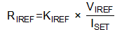
8.2.2 Detailed Design Procedure
LP50xx scales up the reference current (IREF) set by the external resistor (RIREF) to sink the output current (IOUT) at each output port. The following formula can be used to calculate the external resistor (RIREF):
The SCL and SDA lines must each have a pullup resistor placed somewhere on the line (the pullup resistors are normally located on the bus master). In typical applications, values of 1.8kΩ to 4.7kΩ are used.
VCAP is internal LDO output pin. This pin must be connected through a 1µF capacitor to GND. Place the capacitor as close to the device as possible.
TI recommends having a 1µF capacitor between VCC and GND to ensure proper operation. Place the capacitor as close to the device as possible.