JAJSF10C October 2018 – July 2024 LP5018 , LP5024
PRODUCTION DATA
- 1
- 1 特長
- 2 アプリケーション
- 3 概要
- 4 概要 (続き)
- 5 Pin Configuration and Functions
- 6 Specifications
-
7 Detailed Description
- 7.1 Overview
- 7.2 Functional Block Diagram
- 7.3
Feature Description
- 7.3.1 PWM Control for Each Channel
- 7.3.2 LED Bank Control
- 7.3.3 Current Range Setting
- 7.3.4 Automatic Power-Save Mode
- 7.3.5 Protection Features
- 7.4 Device Functional Modes
- 7.5 Programming
- 7.6
Register Maps
- 7.6.1 DEVICE_CONFIG0 (Address = 0h) [reset = 0h]
- 7.6.2 DEVICE_CONFIG1 (Address = 1h) [reset = 3Ch]
- 7.6.3 LED_CONFIG0 (Address = 2h) [reset = 00h]
- 7.6.4 BANK_BRIGHTNESS (Address = 3h) [reset = FFh]
- 7.6.5 BANK_A_COLOR (Address = 4h) [reset = 00h]
- 7.6.6 BANK_B_COLOR (Address = 5h) [reset = 00h]
- 7.6.7 BANK_C_COLOR (Address = 6h) [reset = 00h]
- 7.6.8 LED0_BRIGHTNESS (Address = 7h) [reset = FFh]
- 7.6.9 LED1_BRIGHTNESS (Address = 8h) [reset = FFh]
- 7.6.10 LED2_BRIGHTNESS (Address = 9h) [reset = FFh]
- 7.6.11 LED3_BRIGHTNESS (Address = 0Ah) [reset = FFh]
- 7.6.12 LED4_BRIGHTNESS (Address = 0Bh) [reset = FFh]
- 7.6.13 LED5_BRIGHTNESS (Address = 0Ch) [reset = FFh]
- 7.6.14 LED6_BRIGHTNESS (Address = 0Dh) [reset = FFh]
- 7.6.15 LED7_BRIGHTNESS (Address = 0Eh) [reset = FFh]
- 7.6.16 OUT0_COLOR (Address = 0Fh) [reset = 00h]
- 7.6.17 OUT1_COLOR (Address = 10h) [reset = 00h]
- 7.6.18 OUT2_COLOR (Address = 11h) [reset = 00h]
- 7.6.19 OUT3_COLOR (Address = 12h) [reset = 00h]
- 7.6.20 OUT4_COLOR (Address = 13h) [reset = 00h]
- 7.6.21 OUT5_COLOR (Address = 14h) [reset = 00h]
- 7.6.22 OUT6_COLOR (Address = 15h) [reset = 00h]
- 7.6.23 OUT7_COLOR (Address = 16h) [reset = 00h]
- 7.6.24 OUT8_COLOR (Address = 17h) [reset = 00h]
- 7.6.25 OUT9_COLOR (Address = 18h) [reset = 00h]
- 7.6.26 OUT10_COLOR (Address = 19h) [reset = 00h]
- 7.6.27 OUT11_COLOR (Address = 1Ah) [reset = 00h]
- 7.6.28 OUT12_COLOR (Address = 1Bh) [reset = 00h]
- 7.6.29 OUT13_COLOR (Address = 1Ch) [reset = 00h]
- 7.6.30 OUT14_COLOR (Address = 1Dh) [reset = 00h]
- 7.6.31 OUT15_COLOR (Address = 1Eh) [reset = 00h]
- 7.6.32 OUT16_COLOR (Address = 1Fh) [reset = 00h]
- 7.6.33 OUT17_COLOR (Address = 20h) [reset = 00h]
- 7.6.34 OUT18_COLOR (Address = 21h) [reset = 00h]
- 7.6.35 OUT19_COLOR (Address = 22h) [reset = 00h]
- 7.6.36 OUT20_COLOR (Address = 23h) [reset = 00h]
- 7.6.37 OUT21_COLOR (Address = 24h) [reset = 00h]
- 7.6.38 OUT22_COLOR (Address = 25h) [reset = 00h]
- 7.6.39 OUT23_COLOR (Address = 26h) [reset = 00h]
- 7.6.40 RESET (Address = 27h) [reset = 00h]
- 8 Application and Implementation
- 9 Device and Documentation Support
- 10Revision History
- 11Mechanical, Packaging, and Orderable Information
パッケージ・オプション
メカニカル・データ(パッケージ|ピン)
- RSM|32
サーマルパッド・メカニカル・データ
- RSM|32
発注情報
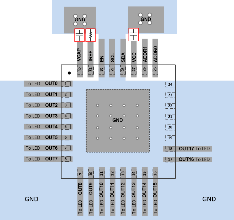
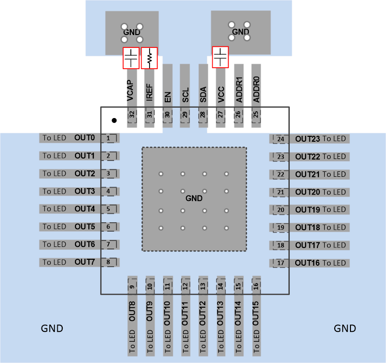
8.4.2 Layout Examples
 Figure 8-4 LP5018 VQFN Layout
Example
 Figure 8-5 LP5024 VQFN Layout
Example
 Figure 8-6 LP5018
VSSOP Layout Example for Single Layer PCB