JAJSF10C October 2018 – July 2024 LP5018 , LP5024
PRODUCTION DATA
- 1
- 1 特長
- 2 アプリケーション
- 3 概要
- 4 概要 (続き)
- 5 Pin Configuration and Functions
- 6 Specifications
-
7 Detailed Description
- 7.1 Overview
- 7.2 Functional Block Diagram
- 7.3
Feature Description
- 7.3.1 PWM Control for Each Channel
- 7.3.2 LED Bank Control
- 7.3.3 Current Range Setting
- 7.3.4 Automatic Power-Save Mode
- 7.3.5 Protection Features
- 7.4 Device Functional Modes
- 7.5 Programming
- 7.6
Register Maps
- 7.6.1 DEVICE_CONFIG0 (Address = 0h) [reset = 0h]
- 7.6.2 DEVICE_CONFIG1 (Address = 1h) [reset = 3Ch]
- 7.6.3 LED_CONFIG0 (Address = 2h) [reset = 00h]
- 7.6.4 BANK_BRIGHTNESS (Address = 3h) [reset = FFh]
- 7.6.5 BANK_A_COLOR (Address = 4h) [reset = 00h]
- 7.6.6 BANK_B_COLOR (Address = 5h) [reset = 00h]
- 7.6.7 BANK_C_COLOR (Address = 6h) [reset = 00h]
- 7.6.8 LED0_BRIGHTNESS (Address = 7h) [reset = FFh]
- 7.6.9 LED1_BRIGHTNESS (Address = 8h) [reset = FFh]
- 7.6.10 LED2_BRIGHTNESS (Address = 9h) [reset = FFh]
- 7.6.11 LED3_BRIGHTNESS (Address = 0Ah) [reset = FFh]
- 7.6.12 LED4_BRIGHTNESS (Address = 0Bh) [reset = FFh]
- 7.6.13 LED5_BRIGHTNESS (Address = 0Ch) [reset = FFh]
- 7.6.14 LED6_BRIGHTNESS (Address = 0Dh) [reset = FFh]
- 7.6.15 LED7_BRIGHTNESS (Address = 0Eh) [reset = FFh]
- 7.6.16 OUT0_COLOR (Address = 0Fh) [reset = 00h]
- 7.6.17 OUT1_COLOR (Address = 10h) [reset = 00h]
- 7.6.18 OUT2_COLOR (Address = 11h) [reset = 00h]
- 7.6.19 OUT3_COLOR (Address = 12h) [reset = 00h]
- 7.6.20 OUT4_COLOR (Address = 13h) [reset = 00h]
- 7.6.21 OUT5_COLOR (Address = 14h) [reset = 00h]
- 7.6.22 OUT6_COLOR (Address = 15h) [reset = 00h]
- 7.6.23 OUT7_COLOR (Address = 16h) [reset = 00h]
- 7.6.24 OUT8_COLOR (Address = 17h) [reset = 00h]
- 7.6.25 OUT9_COLOR (Address = 18h) [reset = 00h]
- 7.6.26 OUT10_COLOR (Address = 19h) [reset = 00h]
- 7.6.27 OUT11_COLOR (Address = 1Ah) [reset = 00h]
- 7.6.28 OUT12_COLOR (Address = 1Bh) [reset = 00h]
- 7.6.29 OUT13_COLOR (Address = 1Ch) [reset = 00h]
- 7.6.30 OUT14_COLOR (Address = 1Dh) [reset = 00h]
- 7.6.31 OUT15_COLOR (Address = 1Eh) [reset = 00h]
- 7.6.32 OUT16_COLOR (Address = 1Fh) [reset = 00h]
- 7.6.33 OUT17_COLOR (Address = 20h) [reset = 00h]
- 7.6.34 OUT18_COLOR (Address = 21h) [reset = 00h]
- 7.6.35 OUT19_COLOR (Address = 22h) [reset = 00h]
- 7.6.36 OUT20_COLOR (Address = 23h) [reset = 00h]
- 7.6.37 OUT21_COLOR (Address = 24h) [reset = 00h]
- 7.6.38 OUT22_COLOR (Address = 25h) [reset = 00h]
- 7.6.39 OUT23_COLOR (Address = 26h) [reset = 00h]
- 7.6.40 RESET (Address = 27h) [reset = 00h]
- 8 Application and Implementation
- 9 Device and Documentation Support
- 10Revision History
- 11Mechanical, Packaging, and Orderable Information
パッケージ・オプション
メカニカル・データ(パッケージ|ピン)
- RSM|32
サーマルパッド・メカニカル・データ
- RSM|32
発注情報
7.5.1.3 Transferring Data
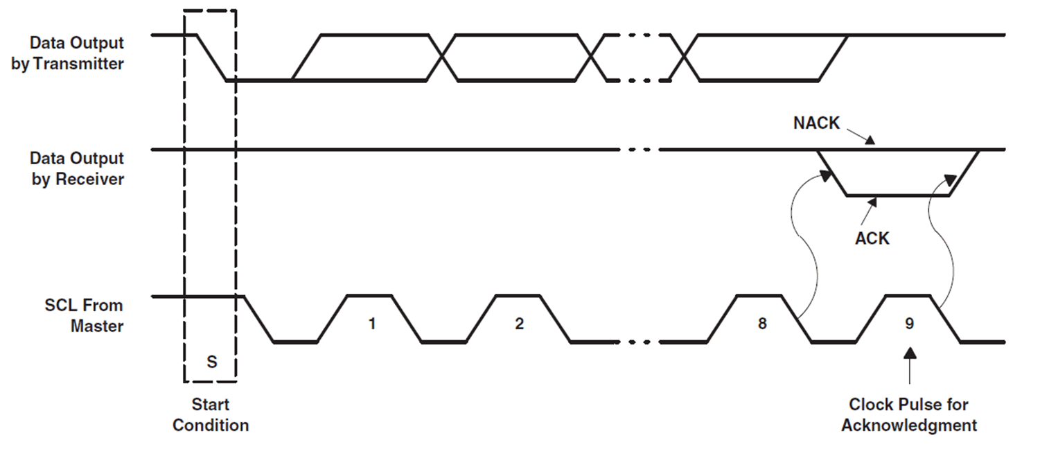
Every byte put on the SDA line must be eight bits long, with the most-significant bit (MSB) being transferred first. Each byte of data must be followed by an acknowledge bit. The acknowledge-related clock pulse is generated by the master. The master releases the SDA line (HIGH) during the acknowledge clock pulse. The device pulls down the SDA line during the ninth clock pulse, signifying an acknowledge. The device generates an acknowledge after each byte has been received.
There is one exception to the acknowledge-after-every-byte rule. When the master is the receiver, it must indicate to the transmitter an end of data by not acknowledging (negative acknowledge) the last byte clocked out of the slave. This negative acknowledge still includes the acknowledge clock pulse (generated by the master), but the SDA line is not pulled down.
After the START condition, the bus master sends a chip address. This address is seven bits long followed by an eighth bit which is a data direction bit (READ or WRITE). For the eighth bit, a 0 indicates a WRITE, and a 1 indicates a READ. The second byte selects the register to which the data is written. The third byte contains data to write to the selected register.
 Figure 7-10 Acknowledge and Not
Acknowledge on I2C Bus