SNVS458D June 2007 – October 2016 LP55281
PRODUCTION DATA.
- 1 Features
- 2 Applications
- 3 Description
- 4 Revision History
- 5 Pin Configuration and Functions
- 6 Specifications
- 7 Detailed Description
- 8 Application and Implementation
- 9 Power Supply Recommendations
- 10Layout
- 11Device and Documentation Support
- 12Mechanical, Packaging, and Orderable Information
7 Detailed Description
7.1 Overview
The LP55281 boost DC-DC converter generates a 4-V to 5.3-V supply voltage for the LEDs from single Li-Ion battery (3 V...4.5 V). The output voltage is controlled with an 8-bit register in 9 steps. The converter is a magnetic switching PWM mode DC-DC converter with a current limit. When timing resistor RT is 82 kΩ, the converter has three options for switching frequency: 1 MHz, 1.67 MHz, and 2 MHz (default). Timing resistor defines the internal oscillator frequency and thus directly affects boost frequency and all internally generated timing (RGB, ALED) of the circuit.
The LP55281 boost converter uses pulse-skipping elimination to stabilize the noise spectrum. Even with light load or no load a minimum length current pulse is fed to the inductor. An active load is used to remove the excess charge from the output capacitor at very light loads. At very light load and when input and output voltages are very close to each other, the pulse skipping is not completely eliminated. Output voltage must be at least 0.5 V higher than input voltage to avoid pulse skipping. Reducing the switching frequency also reduces the required voltage difference.
Active load can be disabled with the EN_AUTOLOAD bit. Disabling increases the efficiency at light loads, but the downside is that pulse skipping will occur. The boost converter must be stopped when there is no load to minimize the current consumption.
The topology of the magnetic boost converter is called current programmed mode (CPM) control, where the inductor current is measured and controlled with the feedback. The user can program the output voltage of the boost converter. The output voltage control changes the resistor divider in the feedback loop.
Figure 10 shows the boost topology with the protection circuitry. Four different protection schemes are implemented:
- Overvoltage protection — limits the maximum output voltage
- Keeps the output below breakdown voltage.
- Prevents boost operation if battery voltage is much higher than desired output.
- Overcurrent protection — limits the maximum inductor current
- Voltage over switching NMOS is monitored; too high voltages turn the switch off.
- Feedback break protection — prevents uncontrolled operation if FB pin gets disconnected.
- Duty cycle limiting, done with digital control.
 Figure 10. Boost Converter Topology
7.2 Functional Block Diagram

7.3 Feature Description
7.3.1 Magnetic Boost DC-DC Converter
7.3.1.1 Boost Standby Mode
User can stop the boost converter operation by writing the Enables register bit EN_BOOST low. When EN_BOOST is written high, the converter starts for 10 ms in PFM mode and then goes to PWM mode.
7.3.1.2 Boost Output Voltage Control
User can control the Boost output voltage by boost output 8-bit register.
| BOOST OUTPUT [7:0] Register 0Fh | BOOST OUTPUT VOLTAGE (TYPICAL) | |
| Bin | Hex | |
| 0000 0000 | 00 | 4 V |
| 0000 0001 | 01 | 4.25 V |
| 0000 0011 | 03 | 4.4 V |
| 0000 0111 | 07 | 4.55 V |
| 0000 1111 | 0F | 4.7 V |
| 0001 1111 | 1F | 4.85 V |
| 0011 1111 | 3F | 5 V (default) |
| 0111 1111 | 7F | 5.15 V |
| 1111 1111 | FF | 5.3 V |
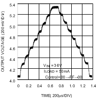 Figure 11. Boost Output Voltage Control
7.3.1.3 Boost Frequency Control
Register-frequency selections (address 10h). Register default value after reset is 07h.
| FRQ_SEL[2:0] | FREQUENCY |
| 1XX | 2 MHz |
| 01X | 1.67 MHz |
| 001 | 1 MHz |
7.3.2 Functionality of RGB LED Outputs (R1-4, G1-4, B1-4)
The LP55281 device has 4 sets of RGB/color LED outputs. Each set has 3 outputs, which can be controlled individually with a 6-bit PWM control register. The pulsed current level for each LED output is set with a single external resistor RRGB and a 2-bit coarse adjustment bit for each LED output (see Table 1 and Table 2).
Table 1. LED Current Level Adjust
| Rx_IPLS[7:6], Gx_IPLS[7:6], Bx_IPLS[7:6] | SINK CURRENT PULSE (IMAX = 100 × 1.23 / RRGB) – IPLS |
| 00 | 0.25 × IMAX |
| 01 | 0.50 × IMAX |
| 10 | 0.75 × IMAX |
| 11 | 1.00 × IMAX |
Table 2. LED PWM Control
| Rx_PWM[5:0], Gx_PWM[5:0], Bx_PWM[5:0] | AVERAGE SINK CURRENT | PULSE RATIO (%) |
| 000 000 | 0 | 0 |
| 000 001 | 1/63 × IPLS | 1.6 |
| 000 010 | 2/63 × IPLS | 3.2 |
| ... | ... | ... |
| 111 110 | 62/63 × IPLS | 98.4 |
| 111 111 | 63/63 × IPLS | 100 |
Each RGB set must be enabled separately by setting EN_RGBx bit to 1. The device must be enabled (NSTBY = 1) before the RGB outputs can be activated.
When any of EN_RGBx bits are set to 1 and NSTBY = 1, the RGB driver takes a certain quiescent current from battery even if all PWM control bits are 0. The quiescent current is dependent on RRGB resistor, and can be calculated from formula IR_RGB = 1.23 V / RRGB.
7.3.2.1 PWM Control Timing
PWM frequency can be selected from 3 predefined values: 10 kHz, 20 kHz, and 40 kHz. The frequency is selected with FPWM1 and FPWM0 bits, see Table 3.
Table 3. PWM Frequency
| FPWM1 | FPWM0 | PWM FREQUENCY (fPWM) |
| 0 | 0 | 9.92 kHz |
| 0 | 1 | 19.84 kHz |
| 1 | 0 | 39.68 kHz |
| 1 | 1 | 39.68 kHz |
Each RGB set has equivalent internal PWM timing between R, G, and B: R has a fixed start time, G has a fixed mid-pulse time, and B has a fixed-pulse end time. PWM start time for each RGB set is different in order to minimize the instantaneous current loading due to the current sink switch on transition. See Figure 12 for details.
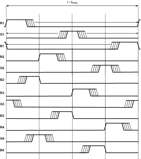 Figure 12. Timing Diagram
7.3.3 Audio Synchronization
The ALED output can be synchronized to incoming audio with an audio-synchronization feature. Audio synchronization synchronizes ALED based on the peak amplitude of the input signal. Programmable gain and automatic gain control function are also available for adjustment of input signal amplitude to light response. Control of ALED brightness refreshing frequency is done with four different frequency configurations. The digitized input signal has DC component that is removed by a digital DC-remover (–3 dB at 500 Hz). LP55281 has a 2-channel audio (stereo) input for audio synchronization, as shown in Figure 13. The inputs accept signals in the range of 0 V to 1.6 V peak-to-peak, and these signals are mixed into a single wave so that they can be filtered simultaneously.
LP55281 audio synchronization is mainly realized digitally, and it consists of the following signal path blocks (see Figure 13):
- Input buffer
- AD converter
- Automatic gain control (AGC) and manually programmable gain
- Peak detector
 Figure 13. ALED Audio Synchronization
7.3.3.1 Control of Audio Synchronization
Table 4 describes the controls required for audio synchronization. ALED brightness control through serial interface is not available when audio synchronization is enabled.
Table 4. Audio Synchronization Control (Registers 0Dh And 0Eh)
| NAME | BIT | DESCRIPTION |
| GAIN_SEL[2:0] | Register 0Dh Bits 7-5 |
Input signal gain control. Gain has a range from 0 dB to -46 dB. [000] = 0 dB, [001] = –6 dB, [010] = –12 dB, [011] = –18 dB, [100] = -24 dB, [101] = -31 dB, [110] = -37 dB, [111] = –46 dB |
| DC_FREQ | Register 0Dh Bit 4 |
Control of the high-pass filter's corner frequency: 0 = 80 Hz 1 = 510 Hz |
| EN_AGC | Register 0Dh Bits 3 |
Automatic gain control. Set EN_AGC = 1 to enable automatic control or 0 to disable. When EN_AGC is disabled, the audio input signal gain value is defined by GAIN_SEL. |
| EN_SYNC | Register 0Dh Bits 2 |
Audio synchronization enabled. Set EN_SYNC = 1 to enable audio synchronization or 0 to disable. |
| SPEED_CTRL[1:0] | Register 0Dh Bits 1-0 |
Control for refreshing frequency. Sets the typical refreshing rate for the ALED output [00] = FASTEST, [01] = 15 Hz, [10] = 7.6 Hz, [11] = 3.8 Hz |
| THRESHOLD[3:0] | Register 0Eh Bits 3-0 |
Control for the audio input threshold. Sets the typical threshold for the audio inputs signals. May be needed if there is noise on the audio lines. |
Table 5. Audio Input Threshold Setting (Register 0Eh)
| THRESHOLD[3:0] | THRESHOLD LEVEL (mV, typical) |
| 0000 | Disabled |
| 0001 | 0.2 |
| 0010 | 0.4 |
| ... | ... |
| 1110 | 2.5 |
| 1111 | 2.7 |
Table 6. Typical Gain Values vs Audio Input Amplitude
| AUDIO INPUT AMPLITUDE mVP-P | GAIN VALUE (dB) |
| 0 to 10 | 0 |
| 0 to 20 | –6 |
| 0 to 40 | –12 |
| 1 to 85 | –18 |
| 3 to 170 | –24 |
| 5 to 400 | –31 |
| 10 to 800 | –37 |
| 20 to 1600 | –46 |
7.3.3.2 ALED Driver
The LP55281 device has a single ALED driver. It is a constant current sink with an 8-bit control. ALED driver can be used as a DC current sink or an audio synchronized current sink. Note, that when the audio synchronization function is enabled, the 8-bit current control register has no effect.
ALED driver is enabled when audio synchronization is enabled (EN_SYNC = 1) or when ALED[7:0] control byte has other than 00h value.
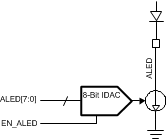 Figure 14. ALED Driver
7.3.3.2.1 Adjustment of ALED Driver
Adjustment of the ALED driver current (Register 0Ch) is described in Table 7.
Table 7. ALED Driver Current
| ALED[7:0] | DRIVER CURRENT, mA (typical) |
| 0000 0000 | 0 |
| 0000 0001 | 0.06 |
| 0000 0010 | 0.1 |
| ... | ... |
| 1111 1101 | 14.8 |
| 1111 1110 | 14.9 |
| 1111 1111 | 15 |
With values other than those in Table 7, the current value can be calculated to be (15 mA / 255) × ALED[7:0], where ALED[7:0] is value in decimals.
 Figure 15. Principle of LED Connection to ADC
7.3.4 LED Test Interface
All LED pin voltages and boost output voltage in LP55281 can be measured and value can be read through the SPI/I2C compatible interface. MUX_LED[3:0] bits in the LED test register (address 12h) are used to select one of the LED outputs or boost output for measurement. The selected output is connected to the internal ADC through a 55-kΩ resistor divider. The AD conversion is activated by setting the EN_LTEST bit to 1. The first conversion is ready after 128 µs from this. The result can be read from the ADC output register (address 13h). The device executes the AD conversions automatically once in every 128 µs period, as long as the EN_LTEST bit is 1.
User can set the preferred DC current level with the LED driver controls. The PWM of the RGB drivers must be set to 100% — otherwise random variation can appear on results. Note that the 55-kΩ resistor divider causes small additional current through the LED under measurement.
ADC result can be converted into a voltage value (of the selected pin) by multiplying the ADC result (in decimals) with 27.345 mV (value of LSB). The calculated voltage value is the voltage between the selected pin and ground. The internal LDO voltage is used as a reference voltage for the conversion. The accuracy of LDO is ± 3%, which is defining the overall accuracy. The non-linearity and offset figures are both better than 2LSB.
Table 8. LED Multiplexing (Register 12h)
| MUX_LED[3:0] | CONNECTION |
| 0000 | R1 |
| 0001 | G1 |
| 0010 | B1 |
| 0011 | R2 |
| 0100 | G2 |
| 0101 | B2 |
| 0110 | R3 |
| 0111 | G3 |
| 1000 | B3 |
| 1001 | R4 |
| 1010 | G4 |
| 1011 | B4 |
| 1100 | ALED |
| 1101 | — |
| 1110 | |
| 1111 | Boost output |
7.3.4.1 LED Test Procedure
An example of LED test sequence is presented here. Note that user can use incremental write sequence on I2C. The test sequence consists of the basic setup and measurement phases for all RGB LEDs and boost voltage.
Basic setup phase for the device:
- Give reset to LP55281 (by power on, NRST pin or write any data to register 60h)
- Set the preferred value for RED1 (write 3Fh, 7Fh, BFh or FFh to register 00h)
- Set the preferred value for GREEN1 (write 3Fh, 7Fh, BFh or FFh to register 01h)
- Set the preferred value for BLUE1 (write 3Fh, 7Fh, BFh or FFh to register 02h)
- Set the preferred value for RED2 (write 3Fh, 7Fh, BFh or FFh to register 03h)
- Set the preferred value for GREEN2 (write 3Fh, 7Fh, BFh or FFh to register 04h)
- Set the preferred value for BLUE2 (write 3Fh, 7Fh, BFh or FFh to register 05h)
- Set the preferred value for RED3 (write 3Fh, 7Fh, BFh or FFh to register 06h)
- Set the preferred value for GREEN3 (write 3Fh, 7Fh, BFh or FFh to register 07h)
- Set the preferred value for BLUE3 (write 3Fh, 7Fh, BFh or FFh to register 08h)
- Set the preferred value for RED4 (write 3Fh, 7Fh, BFh or FFh to register 09h)
- Set the preferred value for GREEN4 (write 3Fh, 7Fh, BFh or FFh to register 0Ah)
- Set the preferred value for BLUE4 (write 3Fh, 7Fh, BFh or FFh to register 0Bh)
- Set the preferred value for ALED (write 01h - FFh to register 0Ch)
- Dummy write: 00h to register 0Dh (Only if the incremental write sequence is used)
- Dummy write: 00h to register 0Eh (Only if the incremental write sequence is used)
- Set preferred boost voltage (write 00h - FFh to register 0Fh)
- Set preferred boost frequency (write 00h - 07h to register 10h, PWM frequency can be anything)
- Enable boost and RGB drivers (write CFh to register 11h)
- Wait 20 ms for the device and boost start-up
Measurement phase:
- Enable LED test and select output (write 1xh to register 12h)
- Wait for 128 µs
- Read ADC output (read register 13h)
- Go to step 1 of measurement phase and define next output to be measured as many times as needed
- Disable LED test (write 00h to register 12h) or give reset to the device (see step 1 in basic setup phase)
7.3.4.2 LED Test Time Estimation
Assuming the maximum clock frequencies used in SPI or I2C-compatible interfaces, Table 9 predicts the overall test sequence time for the test procedure shown above. This estimation gives the shortest time possible. Incremental write is assumed with I2C. Reset and LED test disable are not included.
Table 9. LED Test Time
| TEST PHASE | TIME (ms) | |
|---|---|---|
| I2C | SPI | |
| Setup | 0.528 | 0.024 |
| Boost start-up | 20 | 20 |
| 14 measurements | 4.137 | 1.831 |
| Total time | 24.7 | 21.9 |
7.3.5 7-V Shielding
To shield the LP55281 device from high-input voltages (6 V to 7.2 V), the use of an external 2.8-V LDO is required. This 2.8-V voltage protects internally the device against high voltage condition. The recommended connection is shown in the picture below. Internally both logic and analog circuitry works at 2.8-V supply voltage. Both supply voltage pins should have separate filtering capacitors. TI recommends pulling down the external LDO voltage when it is disabled in order to minimize the leakage current of the LED outputs.
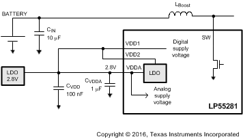 Figure 16. LP55281 With 7-V Shielding
In cases where high voltage is not an issue, the alternative connection is shown below.
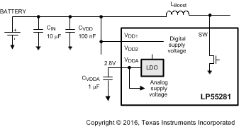 Figure 17. LP55281 Without 7-V Shielding
7.4 Device Functional Modes
7.4.1 Modes Of Operation
-
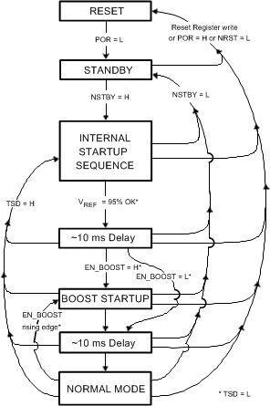
RESET: In the RESET mode all the internal registers are reset to the default values and the device goes to STANDBY mode after reset. NSTBY control bit is low after reset by default. Reset is entered always if Reset Register is written, internal Power On Reset is active, or NRST pin is pulled down externally. The LP55281 can be reset by writing any data to the Reset Register (address 60H). Power On Reset (POR) will activate during the device startup or when the supply voltage VDD2 falls below 1.5 V. Once VDD2 rises above 1.5V, POR inactivates, and the device continues to the STANDBY mode.
-
STANDBY: The STANDBY mode is entered if the register bit NSTBY is LOW. This is the low power consumption mode, when all circuit functions are disabled. Registers can be written in this mode and the control bits are effective immediately after startup.
-
STARTUP: When NSTBY bit is written high, the INTERNAL STARTUP SEQUENCE powers up all the needed internal blocks (VREF, Oscillator, etc.). To ensure the correct oscillator initialization, a 10 ms delay is generated by the internal state-machine. If the device temperature rises too high, the Thermal Shutdown (TSD) disables the device operation and STARTUP mode is entered until no thermal shutdown is present.
-
BOOST STARTUP: Soft start for boost output is generated in the BOOST STARTUP mode. The boost output is raised in PWM mode during the 10 ms delay generated by the state-machine. The Boost startup is entered from Internal Startup Sequence if EN_BOOST is HIGH or from Normal mode when EN_BOOST is written HIGH. During the 10 ms Boost Startup time all LED outputs are switched off to ensure smooth startup.
-
NORMAL: During NORMAL mode the user controls the device using the Control Registers. The registers can be written in any sequence and any number of bits can be altered in a register in one write.
7.5 Programming
The LP55281 supports two different interface modes:
- SPI Interface (4-wire, serial)
- I2C Compatible Serial Bus Interface
User can define the serial interface by IF_SEL pin. If IF_SEL = 0, I2C mode is selected.
7.5.1 SPI Interface
The LP55281 is compatible with SPI serial-bus specification and it operates as a slave. The transmission consists of 16-bit write and read cycles. One cycle consists of a 7 address bits, 1 read/write (RW) bit and 8 data bits. RW bit high state defines a write cycle and low a read cycle. SO output is normally in high-impedance state and it is active only when data is sent out during a read cycle. A pullup resistor may be needed in SO line if a floating logic signal can cause unintended current consumption in the input circuits where SO is connected. The Address and Data are transmitted MSB first. The slave select signal (SS) must be low during the cycle transmission. SS resets the interface when high and it has to be taken high between successive cycles. Data is clocked in on the rising edge of the clock signal (SCK), while data is clocked out on the falling edge of SCK.
 Figure 18. SPI Write Cycle
 Figure 19. SPI Read Cycle
7.5.2 I2C Compatible Serial Bus Interface
7.5.2.1 Interface Bus Overview
The I2C compatible synchronous serial interface provides access to the programmable functions and registers on the device. This protocol uses a two-wire interface for bidirectional communications between the devices connected to the bus. The two interface lines are the serial data line (SDA) and the serial clock line (SCL). These lines should be connected to a positive supply, via a pullup resistor and remain HIGH even when the bus is idle.
For every device on the bus is assigned a unique address and it acts as a master or a slave, depending on whether it generates or receives the SCL. When LP55281 is connected in parallel with other I2C compatible devices, the LP55281 supply voltages VDD1, VDD2 and VDDIO must be active. Supplies are required to make sure that the LP55281 does not disturb the SDA and SCL lines.
7.5.2.2 Data Transactions
One data bit is transferred during each clock pulse. Data is sampled during the high state of the SCL. Consequently, throughout the clock's high period, the data should remain stable. Any changes on the SDA line during the high states of the SCL and in the middle of the transaction, aborts the current transaction. New data should be sent during the low SCL state. This protocol permits a single data line to transfer both command/control information and data using the synchronous serial clock.
 Figure 20. Data Validity
Each data transaction is composed of a start condition, a number of byte transfers (set by the software) and a stop condition to terminate the transaction. Every byte written to the SDA bus must be 8 bits long and is transferred with the most significant bit first. After each byte, an acknowledge signal must follow. The following sections provide further details of this process.
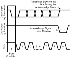 Figure 21. Acknowledge Signal
The Master device on the bus always generates the start and stop conditions (control codes). After a start condition is generated, the bus is considered busy and it retains this status until a certain time after a stop condition is generated. A high-to-low transition of the data line (SDA), while the clock (SCL) is high, indicates a Start Condition. A low-to-high transition of the SDA line, while the SCL is high, indicates a stop condition.
 Figure 22. Start And Stop Conditions
In addition to the first start condition, a repeated start condition can be generated in the middle of a transaction. This allows another device to be accessed or a register read cycle.
7.5.2.3 Acknowledge Cycle
The acknowledge cycle consists of two signals: the acknowledge clock pulse the master sends with each byte transferred, and the acknowledge signal sent by the receiving device.
The master generates the acknowledge clock pulse on the ninth clock pulse of the byte transfer. The transmitter releases the SDA line (permits it to go high) to allow the receiver to send the acknowledge signal. The receiver must pull down the SDA line during the acknowledge clock pulse and ensure that SDA remains low during the high period of the clock pulse, thus signaling the correct reception of the last data byte and its readiness to receive the next byte.
7.5.2.4 Acknowledge After Every Byte Rule
The master generates an acknowledge clock pulse after each byte transfer. The receiver sends an acknowledge signal after every byte received.
There is one exception to theacknowledge after every byte rule. When the master is the receiver, it must indicate to the transmitter an end of data by not-acknowledging (negative acknowledge) the last byte clocked out of the slave. This negative acknowledge still includes the acknowledge clock pulse (generated by the master), but the SDA line is not pulled down.
7.5.2.5 Addressing Transfer Formats
Each device on the bus has a unique slave address. The LP55281 operates as a slave device with 7-bit address. LP55281 I2C address is pin selectable from two different choices. The LP55281 address is 4Ch (SI/A0 = 0) or 4Dh (SI/A0 = 1) as selected with SI/A0 pin. If eighth bit is used for programming, the 8th bit is 1 for read and 0 for write.
Before any data is transmitted, the master transmits the address of the slave being addressed. The slave device should send an acknowledge signal on the SDA line, once it recognizes its address.
The slave address is the first seven bits after a start condition. The direction of the data transfer (R/W) depends on the bit sent after the slave address (the eighth bit).
When the slave address is sent, each device in the system compares this slave address with its own. If there is a match, the device considers itself addressed and sends an acknowledge signal. Depending upon the state of the R/W bit (1 for read, 0 for write), the device acts as a transmitter or a receiver.
 Figure 23. I2C Device Address
7.5.2.6 Control Register Write Cycle
- Master device generates start condition
- Master device sends slave address (7 bits) and the data direction bit (r/w=0).
- Slave device sends acknowledge signal if the slave address is correct.
- Master sends control register address (8 bits).
- Slave sends acknowledge signal.
- Master sends data byte to be written to the addressed register.
- Slave sends acknowledge signal.
- If master will send further data bytes, the control register address will be incremented by one after acknowledge signal
- Write cycle ends when the master creates stop condition.
7.5.2.7 Control Register Read Cycle
- Master device generates a start condition.
- Master device sends slave address (7 bits) and the data direction bit (r/w=0).
- Slave device sends acknowledge signal if the slave address is correct.
- Master sends control register address (8 bits).
- Slave sends acknowledge signal.
- Master device generates repeated start condition.
- Master sends the slave address (7 bits) and the data direction bit (r/w=1).
- Slave sends acknowledge signal if the slave address is correct.
- Slave sends data byte from addressed register.
- If the master device sends acknowledge signal, the control register address will be incremented by one. Slave device sends data byte from addressed register.
- Read cycle ends when the master does not generate acknowledge signal after data byte and generates stop condition.
| ADDRESS MODE | |
| Data Read | <Start Condition> <Slave Address><r/w = 0>[Ack] <Register Address>[Ack] <Repeated Start Condition> <Slave Address><r/w = 1>[Ack] [Register Data]<Ack or NAck> ...additional reads from subsequent register address possible <Stop Condition> |
| Data Write | <Start Condition> <Slave Address><r/w = 0>[Ack] <Register Address>[Ack] <Register Data>[Ack] ...additional writes to subsequent register address possible <Stop Condition> |
< > Data from master, [ ] data from slave
 Figure 24. Register READ Format
When a READ function is to be accomplished, a WRITE function must precede the READ function, as shown in the Read Cycle waveform.
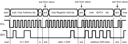 Figure 25. Register WRITE Format
- w = write (SDA = 0)
- r = read (SDA = 1)
- ack = acknowledge (SDA pulled down by either master or slave)
- rs = repeated start
- id = 7-bit device address
7.6 Register Maps
Following table summarizes the registers and their default values
| Address | Register | D7 | D6 | D5 | D4 | D3 | D2 | D1 | D0 |
|---|---|---|---|---|---|---|---|---|---|
| 00h | RED1 | R1 - IPLS[7:6] | R1_PWM[5:0] | ||||||
| 0 | 0 | 0 | 0 | 0 | 0 | 0 | 0 | ||
| 01h | GREEN1 | G1 - IPLS[7:6] | G1_PWM[5:0] | ||||||
| 0 | 0 | 0 | 0 | 0 | 0 | 0 | 0 | ||
| 02h | BLUE1 | B1 - IPLS[7:6] | B1_PWM[5:0] | ||||||
| 0 | 0 | 0 | 0 | 0 | 0 | 0 | 0 | ||
| 03h | RED2 | R2 - IPLS[7:6] | R2_PWM[5:0] | ||||||
| 0 | 0 | 0 | 0 | 0 | 0 | 0 | 0 | ||
| 04h | GREEN2 | G2 - IPLS[7:6] | G2_PWM[5:0] | ||||||
| 0 | 0 | 0 | 0 | 0 | 0 | 0 | 0 | ||
| 05h | BLUE2 | B2 - IPLS[7:6] | B2_PWM[5:0] | ||||||
| 0 | 0 | 0 | 0 | 0 | 0 | 0 | 0 | ||
| 06h | RED3 | R3 - IPLS[7:6] | R3_PWM[5:0] | ||||||
| 0 | 0 | 0 | 0 | 0 | 0 | 0 | 0 | ||
| 07h | GREEN3 | G3 - IPLS[7:6] | G3_PWM[5:0] | ||||||
| 0 | 0 | 0 | 0 | 0 | 0 | 0 | 0 | ||
| 08h | BLUE3 | B3 - IPLS[7:6] | B3_PWM[5:0] | ||||||
| 0 | 0 | 0 | 0 | 0 | 0 | 0 | 0 | ||
| 09h | RED4 | R4 - IPLS[7:6] | R4_PWM[5:0] | ||||||
| 0 | 0 | 0 | 0 | 0 | 0 | 0 | 0 | ||
| 0Ah | GREEN4 | G4 - IPLS[7:6] | G4_PWM[5:0] | ||||||
| 0 | 0 | 0 | 0 | 0 | 0 | 0 | 0 | ||
| 0Bh | BLUE4 | B4 - IPLS[7:6] | B4_PWM[5:0] | ||||||
| 0 | 0 | 0 | 0 | 0 | 0 | 0 | 0 | ||
| 0Ch | ALED | ALED[7:0] | |||||||
| 0 | 0 | 0 | 0 | 0 | 0 | 0 | 0 | ||
| 0Dh | Audio Sync CTRL1 | GAIN_SEL[2:0] | DC_FREQ | EN_AGC | EN_SYNC | SPEED_CTRL[1:0] | |||
| 0 | 0 | 0 | 0 | 0 | 0 | 1 | 1 | ||
| 0Eh | Audio Sync CTRL2 | THRESHOLD[3:0] | |||||||
| 0 | 0 | 0 | 0 | ||||||
| 0Fh | Boost Output | Boost[7:0] | |||||||
| 0 | 0 | 1 | 1 | 1 | 1 | 1 | 1 | ||
| 10h | Frequency Selections | FPWM1 | FPWM0 | FRQ_SEL[2:0] | |||||
| 0 | 0 | 1 | 1 | 1 | |||||
| 11h | Enables | NSTBY | EN_BOOST | EN_AUTOLOAD | EN_RGB4 | EN_RGB3 | EN_RGB2 | EN_RGB1 | |
| 0 | 0 | 0 | 0 | 0 | 0 | 0 | |||
| 12h | LED Test | EN_LTEST | MUX_LED[3:0] | ||||||
| 0 | 0 | 0 | 0 | 0 | |||||
| 13h(1) | ADC Output | DATA[7:0] | |||||||
| 0 | 0 | 0 | 0 | 0 | 0 | 0 | 0 | ||
| r/o | r/o | r/o | r/o | r/o | r/o | r/o | r/o | ||
| 60h | Reset | Writing any data to Reset Register resets LP55281 | |||||||