SNVS873E August 2012 – November 2016 LP5560
PRODUCTION DATA.
- 1 Features
- 2 Applications
- 3 Description
- 4 Revision History
- 5 Pin Configuration and Functions
- 6 Specifications
-
7 Detailed Description
- 7.1 Overview
- 7.2 Functional Block Diagram
- 7.3 Feature Description
- 7.4 Device Functional Modes
- 7.5 Programming
- 7.6 Registers
- 8 Application and Implementation
- 9 Power Supply Recommendations
- 10Layout
- 11Device and Documentation Support
- 12Mechanical, Packaging, and Orderable Information
7 Detailed Description
7.1 Overview
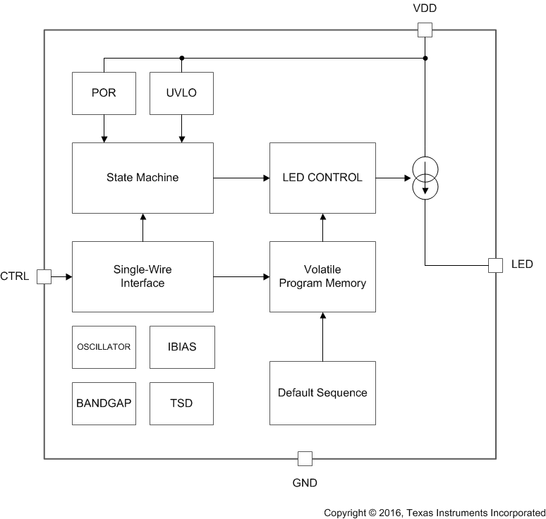
The LP5560 is a programmable LED driver with a single-wire interface. It is designed to drive a single indicator LED with different blinking sequences. Up to three pulses with different on and off times can be programmed into the device. LED current rise and fall times can also be independently controlled. Blinking sequence is stored into volatile memory, thus removing input voltage VIN resets the memory into default state.
The high-side LED driver has very low headroom voltage requirement and can drive most indicator LEDs directly from battery voltage. A single CTRL pin is used to control the device on and off and to change settings of the device. A default blinking sequence is programmed into the LP5560 to enable use of the devices in simply applications without programming capabilities.
7.2 Functional Block Diagram
7.3 Feature Description
7.3.1 LED Driver Headroom Voltage
The current source is connected internally between the VDD and LED output pins. The voltage across the current source, (VVDD − VLED), is referred as headroom voltage (VHR). The current source requires a sufficient amount of headroom voltage to be present across it in order to regulate the output current properly. The LP5560 headroom voltage requirement is 40 mV (typical) and does not depend on the current setting.
7.3.2 Single-Wire Interface
The LP5560 has one digital control input (CTRL). Threshold levels of CTRL input are fixed to support control from low-voltage controller. The CTRL signal is used to control the mode of the circuit. The rising edge of the CTRL signal activates the circuit and starts a command entering period. During the command entering period all rising edges are counted. After command entering period there is a blank period when no rising edges are allowed. If there are any rising edges during blank period these are not detected. User must take care not to start the training sequence before blank period has elapsed or the training sequence is corrupted.
If CTRL is left high after command entering period, the consequent command is performed right after the blank period. In case of run once command CTRL pin can be set low after the command entering period and execution of the command starts once CTRL pin is pulled high after blank period.
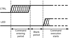 Figure 8. Single-Wire Interface
The LP5560 has four different commands. Command depends on the number of rising edges during command entering period. If there are more than 4 rising edges during command entering period command is ignored. Note that even in this case blank period needs to elapse before next command can be given.
Table 1. LP5560 Commands
| COMMAND | NUMBER OF RISING EDGES DURING COMMAND ENTERING PERIOD |
|---|---|
| Run | 1 |
| Training start | 2 |
| Training end | 3 |
| Run once | 4 |
7.3.2.1 Run Command
One rising edge of the CTRL signal within command entering period is interpreted as a run command. The CTRL pin must be kept high during blank period. If the CTRL pin is pulled low during command entering period or blank period device goes to stand by. In run mode (mode bit = 1) blinking sequence is started right after Blank period and it is repeated as long as CTRL signal is kept high. When the CTRL signal is set low device goes into standby mode (Figure 9).
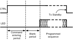 Figure 9. Run Mode
In follow mode (mode bit = 0) LED is turned on right after a blank period, and it stays on as long as CTRL is kept high. When CTRL signal is set low LED is turned off and device goes into standby mode (Figure 10).
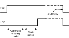 Figure 10. Follow Mode
7.3.2.2 Training Start Command
Two rising edges of CTRL signal within command entering period is interpreted as training start command. Training start command starts training sequence. Different blinking sequences can be trained into device in training mode. Training mode is described in more details in Training Mode.
7.3.2.3 Training End Command
Three rising edges of CTRL signal within command entering period is interpreted as training end command. Training end is used to stop the training sequence.
7.3.2.4 Run-Once Command
Four rising edges of the CTRL signal within command entering period is interpreted as a run-once command. Programmed blinking sequence is performed once after a run-once command. If CTRL is kept high after command entering period the programmed blinking sequence starts right after the blank period has elapsed (Figure 11). The CTRL signal must stay high as long as programmed blinking sequence is executed. If CTRL is set low during execution of blinking sequence, device goes to standby and execution of blinking sequence is stopped.
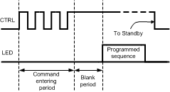 Figure 11. Run-Once Command
If CTRL signal is low after command entering period, blinking sequence is executed once the CTRL is set high (Figure 12).
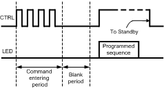 Figure 12. Delayed Run-Once Command
If device is in follow mode (mode bit is 0) the run-once command turns the LED on, and it is kept on as long as CTRL is held high.
7.3.3 Training Mode
Figure 17 shows an example of a full training sequence with three pulses. Training mode starts with a training start command. Training start command is followed by blank time during which no rising edges are allowed. Blank time is followed by calibration pulse. Calibration pulse length (TCAL) defines the speed of the training sequence and can vary from 350 µs to 8 ms. During parameter settings register values are incremented at speed defined by TCAL. For example, if calibration pulse length is 1 ms and current setting pulse length is 3.3 ms, the current-setting value is 3 (current-set register is incremented 3 times). If the parameter-setting pulse is shorter than the calibration pulse, then the corresponding parameter is set to 0.
The next rising edge after calibration pulse starts LED driver current setting (I). LED driver current is recorded once CTRL is pulled low. Note that there are empty low times before and after current setting pulse. For the following pulses both CTRL high and CTRL low times are used to set the parameters. Next the CTRL high time defines the LED current rise time setting for pulse 1 (R1). When R1 setting is started mode bit is set to 0. This sets the LP5560 device into follow mode. Mode bit is set to 1 after first off time has been saved into register. This means that at least one full pulse must be trained into memory to set the device into run mode.
CTRL low time after R1 defines the LED on time for pulse 1 (ON1). CTRL high time after ON1 sets the LED current fall time (F1). CTRL low time after F1 sets pulse 1 off time (OFF1). Once rising edge of CTRL is detected after first off time setting mode bit is set to 1 (run mode) and the number of pulses register (NOP[1:0]) is set to 1. This indicates that one full pulse has been trained into memory.
Rise, on, fall, and off times for pulse 2 and 3 are set the same way as for pulse 1. Note that NOP register is always incremented after OFFx time setting. This means that all pulse parameters (rise, on, fall, and off times) must be trained for each pulse make it valid. The training sequence is ended with training end command.
7.3.3.1 Ending the Training Sequence
A training end command can be given at any time of the training sequence except during blank time. Outcome of the training sequence depends on the place of the training end command. If a training end command is given after any of the off-time setting (OFF1, OFF2 or OFF3), mode bit is set to 1, and the corresponding number of pulses are stored into memory. If a training end command is given after any of the other pulse parameters (Rx, ONx or Fx) that pulse is ignored. For example, if training end command is given after ON2 pulse 2 is ignored and blinking sequence includes only pulse 1.
7.3.3.2 Reset to Default
If a training end command is given right after a training start command, the LP5560 is reset back to factory defaults (Figure 13). In this case the mode bit is set to 1 (run mode) with the factory-set default blinking sequence.
 Figure 13. Reset to Default
7.3.3.3 Changing the LED Current
The LP5560 devices allows changing the LED output current without the need to reprogram the previously programmed blinking sequence. This is done by giving the training end command after current setting (Figure 14). In this case only the current setting changes. If a blinking sequence was programmed into the LP5560 device it remains unchanged. If mode bit was 0 (follow mode) before the training sequence it remains 0.
 Figure 14. Current Programming Sequence
7.3.3.4 Entering Follow Mode
Mode bit can be set to 0 (follow mode) in two ways. If training end command is given after calibration pulse mode bit is set to 0 (follow mode) and the previously set LED output current setting remains unchanged (Figure 15).
 Figure 15. Entering Follow Mode
If training end command is given after R1, ON1 or F1 mode bit is set to 0 (follow mode) and new current setting is stored to current register (Figure 16). If a training end command is given after F1 CTRL low time before training end command needs to be less than minimum training pulse off time (200 µs). Otherwise off time OFF1 is set to minimum value, and pulse 1 is stored into memory.
 Figure 16. Entering Follow Mode With New Current Setting
7.3.3.5 Timeout
If during training CTRL stays constant for more than 127 × TCAL time this is interpreted as timeout. For example, if calibration pulse length TCAL is 1 ms, timeout time is 127 ms. Timeout ends the training sequence. Timeout is considered as a false training, and it is a good practice to always give a complete training sequence after timeout to ensure correct data is stored into memory.
 Figure 17. Full Training Sequence
7.3.4 LED Output Current Setting
The LED output current can be set from 2.8 mA to 19.5 mA in 7 steps. Duration of the current setting pulse (I) defines the current setting.
Table 2. LED Current Setting
| CURRENT SETTING | LED CURRENT (mA) |
|---|---|
| 0 | 2.8 |
| 1 | 5.3 default |
| 2 | 7.8 |
| 3 | 10.2 |
| 4 | 12.6 |
| 5 | 15.0 |
| 6 | 17.3 |
| 7 | 19.5 |
7.3.5 Rise and Fall Time Settings
Rise and fall times of each pulse can be programmed independently. Rise and fall time can be set from 0 to 1584 ms with 105.6 ms steps. Rise and fall times are generated using a combined PWM and current control. Ramp has 32 PWM steps. For the first 8 steps LED current is decreased to 12.5%. For the remaining steps current is set to 100%. Each step is 3.3 ms long. This results in the minimum ramp time of 3.3 ms × 32 = 105.6 ms. When ramp time is increased each PWM step is done multiple times. When setting rise and fall times they are always rounded down. For example if calibration pulse length is 1 ms and rise time setting pulse is 2.9 ms rise time is set to 2 which is 211.2 ms. Rise and fall times can be set to zero by giving pulse that is shorter than calibration pulse.
Table 3. Rise and Fall Time Settings
| RAMP SETTING | RAMP TIME (ms) |
|---|---|
| 0 | 0 |
| 1 | 105.6 |
| 2 | 211.2 |
| 3 | 316.8 |
| 4 | 422.4 |
| 5 | 528 default |
| 6 | 633.6 |
| 7 | 739.2 |
| 8 | 844.8 |
| 9 | 950.4 |
| 10 | 1056 |
| 11 | 1161.6 |
| 12 | 1267.2 |
| 13 | 1372.8 |
| 14 | 1478.4 |
| 15 | 1584 |
7.3.6 LED ON-Time Setting
LED on time has 5-bit control. On time can be controlled from 13.2 ms to 3009.6 ms in 31 steps. Step size is not constant to increase resolution on shorter ON times. With longer on times also the step size is increased. Table 4 shows the available on times.
Table 4. LED ON-Time Setting
| SETTING | LED ON TIME (ms) |
|---|---|
| 0 | 13.2 |
| 1 | 26.4 |
| 2 | 52.8 |
| 3 | 105.6 |
| 4 | 158.4 |
| 5 | 211.2 |
| 6 | 264 |
| 7 | 316.8 |
| 8 | 369.6 |
| 9 | 435.6 |
| 10 | 501.6 default |
| 11 | 594 |
| 12 | 699.6 |
| 13 | 805.2 |
| 14 | 910.8 |
| 15 | 1016.4 |
| 16 | 1122 |
| 17 | 1227.6 |
| 18 | 1353 |
| 19 | 1478.4 |
| 20 | 1603.8 |
| 21 | 1729.2 |
| 22 | 1854.6 |
| 23 | 1980 |
| 24 | 2105.4 |
| 25 | 2230.8 |
| 26 | 2356.2 |
| 27 | 2481.6 |
| 28 | 2613.6 |
| 29 | 2745.6 |
| 30 | 2877.6 |
| 31 | 3009.6 |
7.3.7 LED OFF-Time Setting
LED off time has also 5-bit control. Off time can be controlled from 26.4 ms to 6019.2 ms in 31 steps. Off time is always twice as long as on time with same setting.
Table 5. LED OFF-Time Setting
| SETTING | LED OFF TIME (ms) |
|---|---|
| 0 | 26.4 |
| 1 | 52.8 |
| 2 | 105.6 |
| 3 | 211.2 |
| 4 | 316.8 |
| 5 | 422.4 |
| 6 | 528 |
| 7 | 633.6 |
| 8 | 739.2 |
| 9 | 871.2 |
| 10 | 1003.2 |
| 11 | 1188 |
| 12 | 1399.2 |
| 13 | 1610.4 default |
| 14 | 1821.6 |
| 15 | 2032.8 |
| 16 | 2244 |
| 17 | 2455.2 |
| 18 | 2706 |
| 19 | 2956.8 |
| 20 | 3207.6 |
| 21 | 3458.4 |
| 22 | 3709.2 |
| 23 | 3960 |
| 24 | 4210.8 |
| 25 | 4461.6 |
| 26 | 4712.4 |
| 27 | 4963.2 |
| 28 | 5227.2 |
| 29 | 5491.2 |
| 30 | 5755.2 |
| 31 | 6019.2 |
7.4 Device Functional Modes
-
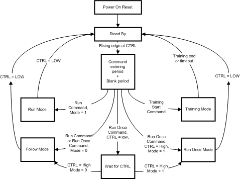
POWER-ON RESET When input voltage is applied to VDD pin device goes through power on reset (POR). During POR defaults are set into control registers.
-
STANDBY: After POR device goes to standby. This is the low power mode when all the internal blocks are shut down.
-
COMMAND ENTERING PERIOD + BLANK PERIOD: Rising edge of the CTRL signal activates the circuit and starts a command entering period. During the command entering period all rising edges are counted. After command entering period there is a blank period when no rising edges are allowed.
-
RUN: If mode bit is 1 (run mode) and run command has been detected device goes into run mode. In run mode LP5560 generates the programmed blinking sequence.
-
FOLLOW MODE: If mode bit is 0 (follow mode) and run command or run once command has been detected LP5560 goes into follow mode. In follow mode LED stays on as long as CTRL pin is held high.
-
RUN-ONCE MODE: If run once command has been detected and mode bit is 1 (run mode) device goes into run-once mode. In run-once mode LP5560 generates the programmed blinking sequence once. CTRL must be high as long as blinking sequence is running.
-
TRAINING: If training start command has been detected device goes into training mode. In training mode a new blinking sequence can be programmed into the device.
7.5 Programming
7.5.1 Default Sequence
Default blinking sequence is programmed into the LP5560 to enable the use of a device in simple systems without programming capabilities. Default sequence has a single pulse with parameters as follows:
I = 5.3 mA; R1 = 528 ms; ON1 = 501.6 ms; F1 = 528; OFF1 = 1610.4 ms
7.6 Registers
7.6.1 Control Registers
Control registers are shown only for a reference. There is no direct way to write or read these registers. Register values are set in the training mode as described earlier in the document.
Table 6. Control Registers
| 7 | 6 | 5 | 4 | 3 | 2 | 1 | 0 |
|---|---|---|---|---|---|---|---|
| F1[3:0] | R1[3:0] | ||||||
| F2[3:0] | R2[3:0] | ||||||
| F3[3:0] | R3[3:0] | ||||||
| MODE | NOP[1:0] | ON1[4:0] | |||||
| I_LED[2:0] | OFF1[4:0] | ||||||
| n/a | ON2[4:0] | ||||||
| n/a | OFF2[4:0] | ||||||
| n/a | ON3[4:0] | ||||||
| n/a | OFF3[4:0] | ||||||