JAJSP11A August 2022 – December 2022 LP5891-Q1
PRODUCTION DATA
- 1 特長
- 2 アプリケーション
- 3 概要
- 4 Revision History
- 5 概要 (続き)
- 6 Pin Configuration and Functions
- 7 Specifications
-
8 Detailed Description
- 8.1 Overview
- 8.2 Functional Block Diagram
- 8.3
Feature Description
- 8.3.1 Independent and Stackable Mode
- 8.3.2 Current Setting
- 8.3.3 Frequency Multiplier
- 8.3.4 Line Transitioning Sequence
- 8.3.5 Protections and Diagnostics
- 8.4 Device Functional Modes
- 8.5 Continuous Clock Series Interface
- 8.6 PWM Grayscale Control
- 8.7 Register Maps
- 9 Application and Implementation
- 10Device and Documentation Support
- 11Mechanical, Packaging, and Orderable Information
パッケージ・オプション
デバイスごとのパッケージ図は、PDF版データシートをご参照ください。
メカニカル・データ(パッケージ|ピン)
- RRF|76
サーマルパッド・メカニカル・データ
発注情報
8.3.4 Line Transitioning Sequence
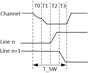
The LP5891-Q1 defines a timing sequence of scan line transition, shown as Figure 8-7. T_SW is the total transitioning time. T_SW is broken up into four intervals: T0 is the time interval between the end of PWM time in current segment and the beginning of channel pre-discharge, T1 is the time interval between the beginning of the channel pre-discharge and the beginning of current line OFF, T2 is the time interval that the beginning of current line OFF and the beginning of next line ON, T3 is the time interval of the beginning of next line ON and the beginning of PWM time in next segment.
 Figure 8-7 Line Transitioning Sequence
The line switch time T_SW equals to T0 + T1 + T2 + T3. T_SW can be configured by the LINE_SWT (see FC1 register bit 40-37 in Table 8-8).
Table 8-4 is the relation between LINE_SWT bits and the line switch time (GCLK numbers) with different internal GCLK frequency.
| LINE_SWT | GCLK Numbers | T_SW (us, 40 MHZ GCLK) | T_SW (us, 60 MHZ GCLK) | T_SW (us, 100 MHZ GCLK) | T_SW (us, 120 MHZ GCLK) | T_SW (us, 160 MHZ GCLK) |
|---|---|---|---|---|---|---|
| 0000b | 45 | 1.125 | 0.7515 | 0.45 | 0.3735 | 0.2835 |
| 0001b | 60 | 1.5 | 1.002 | 0.6 | 0.498 | 0.378 |
| 0010b | 90 | 2.25 | 1.503 | 0.9 | 0.747 | 0.567 |
| 0011b | 120 | 3 | 2.004 | 1.2 | 0.996 | 0.756 |
| 0100b | 150 | 3.75 | 2.505 | 1.5 | 1.245 | 0.945 |
| 0101b | 180 | 4.5 | 3.006 | 1.8 | 1.494 | 1.134 |
| 0110b | 210 | 5.25 | 3.507 | 2.1 | 1.743 | 1.323 |
| 0111b | 240 | 6 | 4.008 | 2.4 | 1.992 | 1.512 |
| 1000b | 270 | 6.75 | 4.509 | 2.7 | 2.241 | 1.701 |
| 1001b | 300 | 7.5 | 5.01 | 3 | 2.49 | 1.89 |
| 1010b | 330 | 8.25 | 5.511 | 3.3 | 2.739 | 2.079 |
| 1011b | 360 | 9 | 6.012 | 3.6 | 2.988 | 2.268 |
| 1100b | 390 | 9.75 | 6.513 | 3.9 | 3.237 | 2.457 |
| 1101b | 420 | 10.5 | 7.014 | 4.2 | 3.486 | 2.646 |
| 1110b | 450 | 11.25 | 7.515 | 4.5 | 3.735 | 2.835 |
| 1111b | 480 | 12 | 8.016 | 4.8 | 3.984 | 3.024 |