SNVS469F October 2006 – December 2015 LP5952
PRODUCTION DATA.
- 1 Features
- 2 Applications
- 3 Description
- 4 Revision History
- 5 Pin Configuration and Functions
-
6 Specifications
- 6.1 Absolute Maximum Ratings
- 6.2 ESD Ratings
- 6.3 Recommended Operating Conditions
- 6.4 Thermal Information
- 6.5 Electrical Characteristics
- 6.6 Electrical Characteristics: Quiescent Currents
- 6.7 Electrical Characteristics: Shutdown Currents
- 6.8 Electrical Characteristics: Enable Control
- 6.9 Electrical Characteristics: Thermal Protection
- 6.10 Electrical Characteristics: Transient Characteristics
- 6.11 Input and Output Capacitors (Recommended)
- 6.12 Typical Characteristics
- 7 Detailed Description
- 8 Application and Implementation
- 9 Power Supply Recommendations
- 10Layout
- 11Device and Documentation Support
- 12Mechanical, Packaging, and Orderable Information
パッケージ・オプション
メカニカル・データ(パッケージ|ピン)
サーマルパッド・メカニカル・データ
発注情報
7 Detailed Description
7.1 Overview
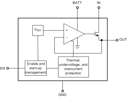
The LP5952 is a dual-supply-rail linear regulator optimized for powering ultralow-voltage circuits from a single Li-Ion cell or 3 cell NiMH/NiCd batteries. In a typical application, BATT is connected to the battery, and IN can be supplied by the output of front stage DC-DC Converter. IN does not exceed BATT at any time.
7.2 Functional Block Diagram

7.3 Feature Description
7.3.1 Dual-Rail Supply
The LP5952 requires two different supply voltages:
- VIN, the power input voltage, is regulated to the fixed output voltage.
- VBATT, the bias input voltage, supplies internal circuitry.
It is important that VIN does not exceed VBATT at any time. If the device is used in the typical post-regulation application as shown in Figure 18, the sequencing of the two power supplies is not an issue because VBATT supplies both the DC-DC regulator and the LP5952 device. The output voltage of the DC-DC regulator takes some time to rise up and supply the input voltage of the device. In this application VIN always ramps up more slowly than VBATT.
If VIN is shorted to VBATT, the voltages at the two supply pins ramp up simultaneously causing no problems.
However, in applications with two independent supplies connected to the LP5952, special care must be taken to ensure that VIN is always ≤ VBATT.
7.3.2 No-Load Stability
The LP5952 remains stable and in regulation with no external load. This is an important consideration in some circuits, for example, CMOS RAM keep-alive applications.
7.3.3 Fast Turnon
Fast turnon is ensured by an optimized architecture allowing a fast ramp of the output voltage to reach the target voltage while the inrush current is controlled low at 120 mA typical (for a COUT of 2.2 µF).
7.3.4 Short-Circuit Protection
The LP5952 is short-circuit protected and, in the event of a peak overcurrent condition, the output current through the NFET pass device is limited.
If the overcurrent condition exists for a longer time, the average power dissipation increases depending on the input-to-output voltage difference until the thermal shutdown circuitry turns the NFET off. Refer to Power Dissipation and Device Operation for power dissipation calculations.
7.3.5 Thermal-Overload Protection
Thermal-overload protection limits the total power dissipation in the LP5952. When the junction temperature exceeds TJ = 165°C typical, the shutdown logic is triggered, and the NFET is turned off, allowing the device to cool down. After the junction temperature dropped by 20°C (temperature hysteresis) typical, the NFET is activated again. This results in a pulsed output voltage during continuous thermal-overload conditions.
The thermal-overload protection is designed to protect the LP5952 in the event of a fault condition. For normal continuous operation, do not exceed the absolute maximum junction temperature rating of TJ = 150°C (see Absolute Maximum Ratings).
7.3.6 Reverse Current Path
The internal NFET pass device in LP5952 has an inherent parasitic body diode. During normal operation, the input voltage is higher than the output voltage, and the parasitic diode is reverse biased. However, if the output is pulled above the input in an application, the current flows from the output to the input as the parasitic diode gets forward biased. The output can be pulled above the input as long as the current in the parasitic diode is limited to 50 mA. For currents above this limit an external Schottky diode must be connected from VOUT to VIN (cathode on VIN, anode on VOUT).
7.4 Device Functional Modes
7.4.1 Enable Operation
The LP5952 may be switched to an ON or OFF state by a logic input at the EN pin, VEN. A logic high at this pin turns the device on. When the enable pin is low, the regulator output is off, and the device typically consumes 0.1 µA.
If the application does not require the enable switching feature, the EN pin must be tied to VBATT to keep the regulator output permanently on.
To ensure proper operation, the signal source used to drive the EN input must be able to swing above and below the specified turnon and turnoff voltage thresholds shown in VIL and VIH in Electrical Characteristics: Enable Control.