SNVS469F October 2006 – December 2015 LP5952
PRODUCTION DATA.
- 1 Features
- 2 Applications
- 3 Description
- 4 Revision History
- 5 Pin Configuration and Functions
-
6 Specifications
- 6.1 Absolute Maximum Ratings
- 6.2 ESD Ratings
- 6.3 Recommended Operating Conditions
- 6.4 Thermal Information
- 6.5 Electrical Characteristics
- 6.6 Electrical Characteristics: Quiescent Currents
- 6.7 Electrical Characteristics: Shutdown Currents
- 6.8 Electrical Characteristics: Enable Control
- 6.9 Electrical Characteristics: Thermal Protection
- 6.10 Electrical Characteristics: Transient Characteristics
- 6.11 Input and Output Capacitors (Recommended)
- 6.12 Typical Characteristics
- 7 Detailed Description
- 8 Application and Implementation
- 9 Power Supply Recommendations
- 10Layout
- 11Device and Documentation Support
- 12Mechanical, Packaging, and Orderable Information
パッケージ・オプション
メカニカル・データ(パッケージ|ピン)
サーマルパッド・メカニカル・データ
発注情報
10 Layout
10.1 Layout Guidelines
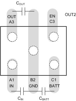
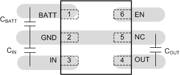
For best overall performance, place all circuit components on the same side of the circuit board and as near to the respective LDO pin connections as practical. Place ground return connections as close as possible to the input and output capacitor and to the LDO ground pin, connected by a wide, copper surface. The use of vias and long traces to create LDO circuit connection is strongly discouraged and negatively affect system performance.
10.2 Layout Examples
 Figure 19. LP5952 DSBGA Layout Example
 Figure 20. LP5952 WSON Layout Example