SNVS469F October 2006 – December 2015 LP5952
PRODUCTION DATA.
- 1 Features
- 2 Applications
- 3 Description
- 4 Revision History
- 5 Pin Configuration and Functions
-
6 Specifications
- 6.1 Absolute Maximum Ratings
- 6.2 ESD Ratings
- 6.3 Recommended Operating Conditions
- 6.4 Thermal Information
- 6.5 Electrical Characteristics
- 6.6 Electrical Characteristics: Quiescent Currents
- 6.7 Electrical Characteristics: Shutdown Currents
- 6.8 Electrical Characteristics: Enable Control
- 6.9 Electrical Characteristics: Thermal Protection
- 6.10 Electrical Characteristics: Transient Characteristics
- 6.11 Input and Output Capacitors (Recommended)
- 6.12 Typical Characteristics
- 7 Detailed Description
- 8 Application and Implementation
- 9 Power Supply Recommendations
- 10Layout
- 11Device and Documentation Support
- 12Mechanical, Packaging, and Orderable Information
パッケージ・オプション
メカニカル・データ(パッケージ|ピン)
サーマルパッド・メカニカル・データ
発注情報
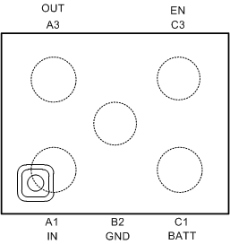
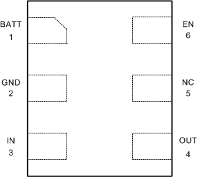
5 Pin Configuration and Functions
YZR Package
5-Pin DSBGA
Top View

NKH Package
6-Pin USON
Top View

NC - No internal connection
Pin Functions
| PIN | TYPE | DESCRIPTION | ||
|---|---|---|---|---|
| NAME | USON | DSGBA | ||
| BATT | 1 | C1 | Input | Bias input voltage; input range: 2.5 V to 5.5 V |
| EN | 6 | C3 | Input | Enable pin logic input: low = shutdown, high = active, normal operation. This pin should not be left floating. Tie to BATT if this function is not used. |
| GND | 2 | B2 | Ground | Ground |
| IN | 3 | A1 | Input | Power input voltage; input range: 0.7 V to 4.5 V, VIN ≤ VBATT |
| NC | 5 | — | — | Do not make connections to this pin. |
| OUT | 4 | A3 | Output | Regulated output voltage |