LP8551 High-Efficiency LED Backlight Driver for Notebooks
1 Features
- High-Voltage DC/DC Boost Converter with Integrated FET; Four Switching Frequency Options: 156/312/625/1250 kHz
- 2.7-V to 22-V Input Voltage Range to Support 1x to 5x Cell Li-Ion Batteries
- 50-mA High-Precision LED Current Sinks
- Adaptive LED Current Sink Headroom Control for Maximum System Efficiency
- Programmable PWM Resolution 8 to 13 Bits
- I2C and PWM Input Duty Cycle Brightness Control
- PWM Output Frequency and LED Current Set Through Resistors
- 4 LED Outputs with LED Fault (short/open) Detection
- Low Input Voltage, Overtemperature, Overcurrent Detection, and Shutdown
- Minimum Number of External Components
2 Applications
- Notebook and Tablet LCD Display LED Backlight
- LED Lighting
3 Description
The LP8551 is a white LED driver with integrated boost converter. It has four adjustable current sinks which can be controlled by PWM input or with I2C-compatible serial interface.
The boost converter has adaptive output voltage control based on the LED driver voltages. This feature minimizes the power consumption by adjusting the voltage to lowest sufficient level in all conditions.
LED outputs have 8-bit current resolution and up to 13-bit PWM resolution to achieve smooth and precise brightness control. Proprietary Phase Shift PWM control is used for LED outputs to reduce peak current from the boost converter, thus making the boost capacitors smaller. The Phase Shifting scheme also eliminates audible noise.
Internal EEPROM is used for storing the configuration data. This makes it possible to have minimum external component count and make the solution very small.
The LP8551 has safety features which make it possible to detect LED outputs with open or short fault. As well, low input voltage and boost overcurrent conditions are monitored, and chip is turned off in case of these events. Thermal de-rating function prevents overheating of the device by reducing backlight brightness when set temperature has been reached.
Device Information(1)
| PART NUMBER | PACKAGE | BODY SIZE (MAX) |
|---|---|---|
| LP8551 | DSBGA (25) | 2.49 mm x 2.49 mm |
- For all available packages, see the orderable addendum at the end of the datasheet.
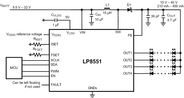
Simplified Schematic
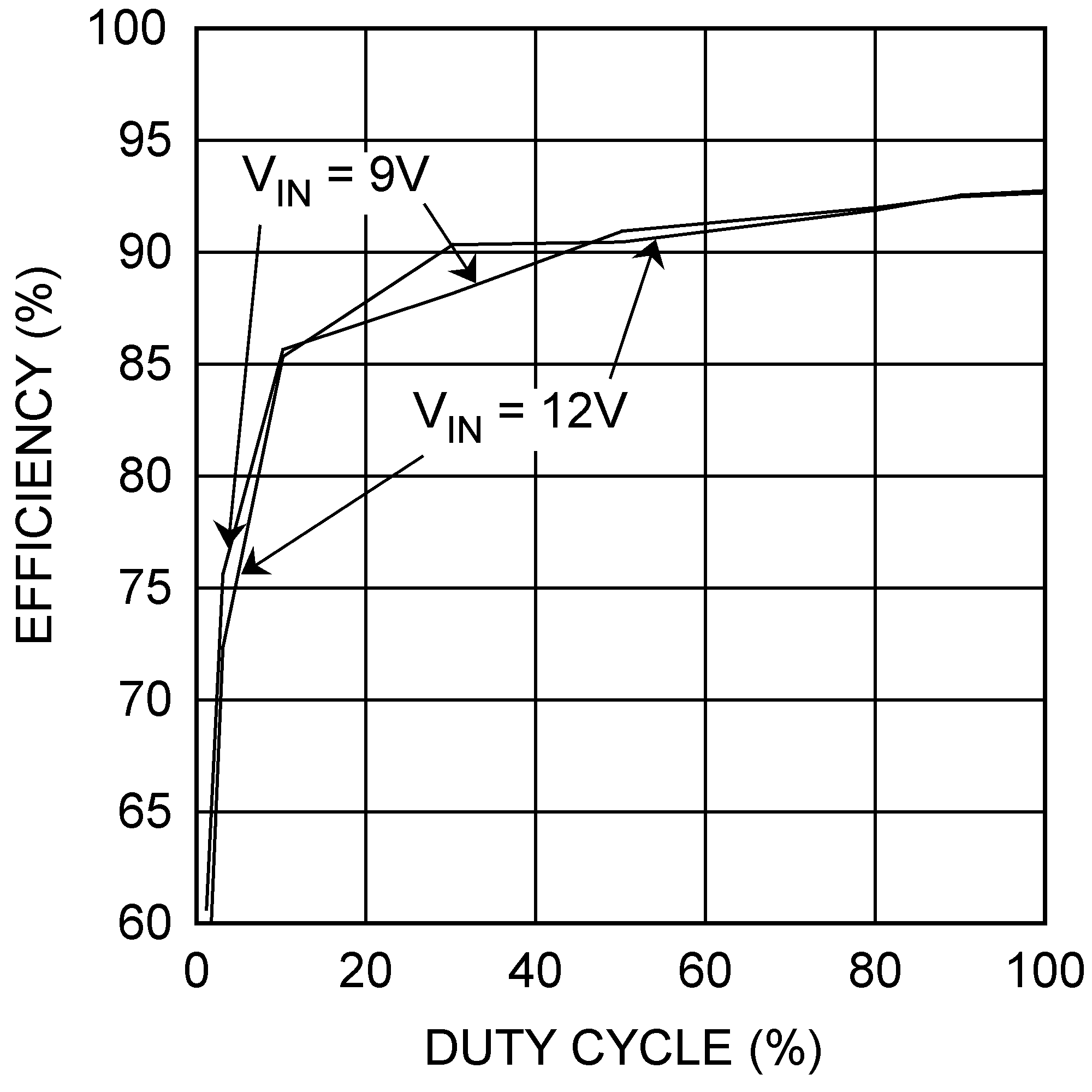
LED Drive Efficiency
4 Revision History
Changes from D Revision (January 2014) to E Revision
- Changed formatting to match new TI datasheet guidelines; added Device Information and Handling Ratings tables, Layout, and Device and Documentation Support sections; reformatted Functional Description to Detailed Description and Applications to Applications and Implementation sections, added note to beginning of Apps & Implementations section; moved some waveforms to new Applications Plots subsection. Go
Changes from C Revision (April 2013) to D Revision
5 Device Default Values
Table 1. Default EEPROM Memory Values
| ADDRESS | DEFAULT VALUES LP8551 |
|---|---|
| A0H | 0111 1111 |
| A1H | 1011 0101 |
| A2H | 1010 1110 |
| A3H | 0111 1011 |
| A4H | 0010 0000 |
| A5H | 0000 1001 |
| A6H | 0000 0000 |
| A7H | 0000 0101 |
6 Pin Configuration and Functions
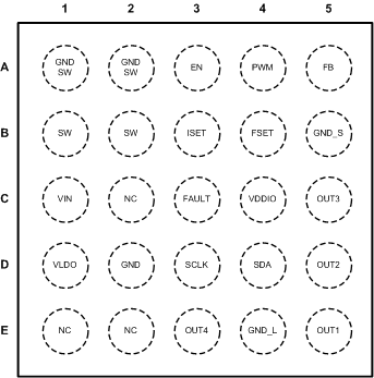
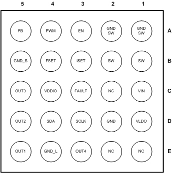
Pin Functions
| PIN | TYPE(1) | DESCRIPTION | |
|---|---|---|---|
| NUMBER | NAME | ||
| A1 | GND_SW | G | Boost switch ground |
| A2 | GND_SW | G | Boost switch ground |
| A3 | EN | I | Enable input pin |
| A4 | PWM | A | PWM dimming input. This pin must be connected to GND if not used. |
| A5 | FB | A | Boost feedback input |
| B1 | SW | A | Boost switch |
| B2 | SW | A | Boost switch |
| B3 | ISET | A | Set resistor for LED current. This pin can be left floating if not used. |
| B4 | FSET | A | PWM frequency set resistor. This pin can be left floating if not used. |
| B5 | GND_S | G | Signal ground |
| C1 | VIN | P | Input power supply up to 22 V. If 2.7 V ≤ VBATT < 5.5 V (Figure 25) then an external 5-V rail must be used for VLDO and VIN. |
| C2 | NC | - | Not connected |
| C3 | FAULT | OD | Fault indication output. If not used, can be left floating. |
| C4 | VDDIO | P | Digital IO reference voltage (1.65 V to 5 V) for I2C interface. If brightness is controlled with PWM input pin then this pin can be connected to GND. |
| C5 | OUT3 | A | Current sink output |
| D1 | VLDO | P | LDO output voltage. External 5-V rail can be connected to this pin in low voltage application. |
| D2 | GND | G | Ground |
| D3 | SCLK | I | Serial clock. This pin must be connected to GND if not used. |
| D4 | SDA | I/O | Serial data. This pin must be connected to GND if not used. |
| D5 | OUT2 | A | Current sink output |
| E1 | NC | - | Not connected |
| E2 | NC | - | Not connected |
| E3 | OUT4 | A | Current sink output |
| E4 | GND_L | G | LED ground |
| E5 | OUT1 | A | Current sink output |