SNVSA15B December 2013 – December 2015 LP8557
PRODUCTION DATA.
- 1 Features
- 2 Applications
- 3 Description
- 4 Revision History
- 5 Device Comparison Table
- 6 Pin Function and Configurations
-
7 Specifications
- 7.1 Absolute Maximum Ratings
- 7.2 ESD Ratings
- 7.3 Recommended Operating Conditions
- 7.4 Thermal Information
- 7.5 Electrical Characteristics
- 7.6 Boost Converter Electrical Characteristics
- 7.7 LED Driver Electrical Characteristics (LED1 To LED6 Pins)
- 7.8 PWM Interface Characteristics (PWM Pin)
- 7.9 Logic Interface Characteristics (PWM, FSET/SDA, ISET/SCL Pins)
- 7.10 I2C Serial Bus Timing Parameters (SDA, SCL)
- 7.11 Typical Characteristics
-
8 Detailed Description
- 8.1 Overview
- 8.2 Functional Block Diagram
- 8.3 Feature Description
- 8.4 Device Functional Modes
- 8.5 Programming
- 8.6 Register Maps
- 9 Application and Implementation
- 10Power Supply Recommendations
- 11Layout
- 12Device and Documentation Support
- 13Mechanical, Packaging, and Orderable Information
7 Specifications
7.1 Absolute Maximum Ratings
Over operating free-air temperature range (unless otherwise noted) (1)(2)| MIN | MAX | UNIT | ||
|---|---|---|---|---|
| VDD | Voltage range on VDD pin | –0.3 | 6 | V |
| VIO | Voltage range on digital IO pins | –0.3 | 6 | V |
| VO | Voltage range on SW, FB, LED1 to LED6 pins | –0.3 | 31 | V |
| TJ | Junction temperature | –30 | 125 | °C |
| Tsldr | Maximum lead temperature (soldering) | 260 | °C | |
| Tstg | Storage temperature range | –65 | 150 | °C |
(1) Stresses beyond those listed under Absolute Maximum Ratings may cause permanent damage to the device. These are stress ratings only, which do not imply functional operation of the device at these or any other conditions beyond those indicated under Recommended Operating Conditions. Exposure to absolute-maximum-rated conditions for extended periods may affect device reliability.
7.2 ESD Ratings
| VALUE | UNIT | |||
|---|---|---|---|---|
| V(ESD) | Electrostatic discharge | Human-body model (HBM), per ANSI/ESDA/JEDEC JS-001(1) | ±2000 | V |
| Charged-device model (CDM), per JEDEC specification JESD22-C101(2) | ±500 | |||
(1) JEDEC document JEP155 states that 500-V HBM allows safe manufacturing with a standard ESD control process.
7.3 Recommended Operating Conditions
Over operating free-air temperature range (unless otherwise noted) (1)(2)| MIN | MAX | UNIT | ||
|---|---|---|---|---|
| VDD | 2.7 | 5.5 | V | |
| V (SW, FB, LED1 to LED6) | 0 | 28 | V | |
| Ambient temperature, TA | –30 | 85 | °C | |
| Junction temperature, TJ | –30 | 125 | °C | |
(1) Stresses beyond those listed under absolute maximum ratings may cause permanent damage to the device. These are stress ratings only, and functional operation of the device at these or any other conditions beyond those indicated under recommended operating conditions is not implied. Exposure to absolute-maximum-rated conditions for extended periods may affect device reliability
(2) All voltage values are with respect to the potential at the GND pin.
7.4 Thermal Information
| THERMAL METRIC(1)(2) | LP8557/LP8557I | UNIT | |
|---|---|---|---|
| YFQ (DSBGA) | |||
| 16 PINS | |||
| RθJA | Junction-to-ambient thermal resistance | 75.7 | °C/W |
| RθJC(top) | Junction-to-case (top) thermal resistance | 0.5 | °C/W |
| RθJB | Junction-to-board thermal resistance | 16.2 | °C/W |
| ψJT | Junction-to-top characterization parameter | 0.2 | °C/W |
| ψJB | Junction-to-board characterization parameter | 16.2 | °C/W |
(1) For more information about traditional and new thermal metrics, see the Semiconductor and IC Package Thermal Metrics application report, SPRA953.
7.5 Electrical Characteristics
Unless otherwise specified: TA = 25°C, VDD = 3.8 V.| PARAMETER | TEST CONDITIONS | MIN | TYP | MAX | UNIT | |
|---|---|---|---|---|---|---|
| VDD | Input voltage range | 2.7 | 5.5 | V | ||
| IDDQ | Standby current | 1 | µA | |||
| IDD | Operating current | No current going through LEDs | 2.2 | mA | ||
| ƒOSC | Internal oscillator frequency accuracy | –4% –7%(1) |
4% 7%(1) |
|||
| TTSD | Thermal shutdown threshold(3) | 150 | °C | |||
| TTSD_hyst | Thermal shutdown hysteresis(3) | 20 | ||||
(1) Limits apply over the full operating ambient temperature range –30°C ≤ TA ≤ 85°C.
7.6 Boost Converter Electrical Characteristics
Unless otherwise specified: TA = 25°C, VDD = 3.8 V(1).| PARAMETER | TEST CONDITIONS | MIN | TYP | MAX | UNIT | |
|---|---|---|---|---|---|---|
| RDS_ON | Switch ON resistance | ISW = 0.5 A | 0.2 | Ω | ||
| VBOOST_MIN | Minimum output voltage | 6(2) | 7 | 8(2) | V | |
| VBOOST_MAX | Maximum output voltage | 27(2) | 28 | 29(2) | V | |
| ISW_CL | SW pin current limit | 2.1 | 2.4 | 2.5 | A | |
| ILOAD_MAX | Maximum continuous load current (3) | ISW_LIM = 2.4 A VIN = 3 V, VOUT = 24 V |
160 | mA | ||
| ƒSW | Switching frequency | 500 1000 |
kHz | |||
| VOVP_TH | Overvoltage protection voltage threshold | VBOOST_MAX
+ 1.6 |
V | |||
| VUVLO_TH | UVLO threshold | 2.5 | ||||
| VUVLO_hyst | UVLO hysteresis | 50 | mV | |||
| tPULSE | Switch pulse minimum width (3) | No load | 80 | ns | ||
| tSTARTUP | Boost start-up time (3) | 1 | ms | |||
(1) Minimum (Min) and Maximum (Max) limits are specified by design, test, or statistical analysis.
(2) Limits apply over the full operating ambient temperature range –30°C ≤ TA ≤ 85°C.
(3) Verified by design and not tested in production.
7.7 LED Driver Electrical Characteristics (LED1 To LED6 Pins)
Unless otherwise specified: TA = 25°C, VDD = 3.8 V(1).| PARAMETER | TEST CONDITIONS | MIN | TYP | MAX | UNIT | |
|---|---|---|---|---|---|---|
| ILEAKAGE | Leakage current | Outputs LED1...LED6, VOUT = 28 V | 1 | µA | ||
| ILED_MAX | Maximum sink current LED1...6 | 25 | mA | |||
| ILED_ACC | LED current accuracy(2) | Output current set to 20 mA | –3% –4%(3) |
3% 4%(3) |
||
| IMATCH | Channel to Channel Matching (2) | Output current set to 20 mA | 0.5 | |||
| ƒLED | LED switching frequency(3) | PFREQ = 000b PFREQ = 111b |
4.9 39.1 |
kHz | ||
| VSAT | Saturation voltage(4) | Output current set to 20 mA | 200 | mV | ||
(1) Minimum (Min) and Maximum (Max) limits are specified by design, test, or statistical analysis.
(2) The LED current accuracy is defined as 100 × (ILED_AVE – ILED_Target) / ILED_AVE. The channel-to-channel LED current matching is defined as (ILED_MAX – ILED_MIN) / ILED_AVE.
(3) Limits apply over the full operating ambient temperature range –30°C ≤ TA ≤ 85°C.
(4) Saturation voltage is defined as the voltage when the LED current has dropped 10% from the value measured at 1 V.
7.8 PWM Interface Characteristics (PWM Pin)
See (1)| PARAMETER | TEST CONDITIONS | MIN | TYP | MAX | UNIT | |
|---|---|---|---|---|---|---|
| ƒPWM | PWM frequency(2) | 75 | 25000 | Hz | ||
| tMIN_ON | Minimum pulse ON time(2) | 1 | µs | |||
| tMIN_OFF | Minimum pulse OFF time(2) | 1 | µs | |||
| tON | Turnon delay from standby to backlight on(2) | PWM pin goes from low to switching. | 9 | ms | ||
| tSTBY | Turnoff delay from backlight off to standby(2) | PWM pin goes from switching to low. | 52 | ms | ||
| PWMRES | PWM input resolution(2) | ƒIN < 2.4 kHz | 12 | bits | ||
| ƒIN < 4.8 kHz | 11 | |||||
| ƒIN < 9.6 kHz | 10 | |||||
| ƒIN < 19.5 kHz | 9 | |||||
| ƒIN < 25 kHz | 8 | |||||
(1) Minimum (Min) and Maximum (Max) limits are specified by design, test, or statistical analysis.
(2) Verified by design and not tested in production.
7.9 Logic Interface Characteristics
(PWM, FSET/SDA, ISET/SCL Pins)
Limits apply over the full operating ambient temperature range –30°C ≤ TA ≤ 85°C(1).
| PARAMETER | TEST CONDITIONS | MIN | TYP | MAX | UNIT | |
|---|---|---|---|---|---|---|
| VIL | Input low level | 0.4 | V | |||
| VIH | Input high level | 1.44 | V | |||
| II | Input current | –1 | 1 | µA | ||
| VOL | Output low level | ISDA = 3 mA | 0.5 | V | ||
| IO | Output leakage | VSDA = 2.8 V | 1 | µA | ||
(1) Minimum (Min) and Maximum (Max) limits are specified by design, test, or statistical analysis.
7.10 I2C Serial Bus Timing Parameters (SDA, SCL)
See(1) and Figure 1.| PARAMETER | MIN | MAX | UNIT | |
|---|---|---|---|---|
| ƒSCL | Clock Frequency | 400 | kHz | |
| 1 | Hold Time (repeated) START Condition | 0.6 | μs | |
| 2 | Clock Low Time | 1.3 | μs | |
| 3 | Clock High Time | 600 | ns | |
| 4 | Setup Time for a Repeated START Condition | 600 | ns | |
| 5 | Data Hold Time | 50 | ns | |
| 6 | Data Setup Time | 100 | ns | |
| 7 | Rise Time of SDA and SCL | 20 + 0.1Cb | 300 | ns |
| 8 | Fall Time of SDA and SCL | 15 + 0.1Cb | 300 | ns |
| 9 | Set-up Time for STOP condition | 600 | ns | |
| 10 | Bus Free Time between a STOP and a START Condition | 1.3 | μs | |
| Cb | Capacitive Load Parameter for Each Bus Line Load of 1 pF corresponds to 1 ns. |
10 | 200 | ns |
| tWAIT | Wait time from VDD = 2.7 V to 1st I2C command | 150 | μs | |
(1) Verified by design and not tested in production.
 Figure 1. I2C-Compatible Timing
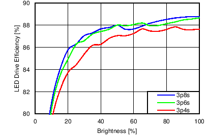
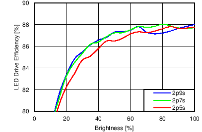
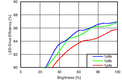
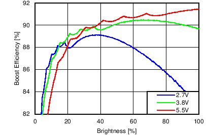
7.11 Typical Characteristics
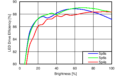
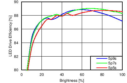
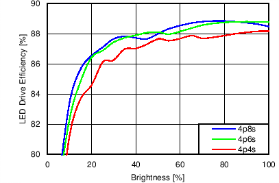
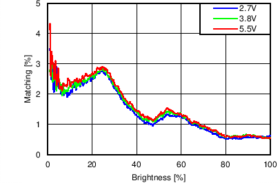
Unless otherwise specified: VIN = VDD = 3.8 V, L = 10 µH Cyntec PIME051E, D = Diodes PD3S130L-7, COUT = 2 × 4.7 µF, LED Vƒ = 2.85 V (typical), ILED_MAX = 25 mA per string.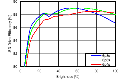
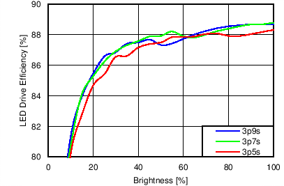
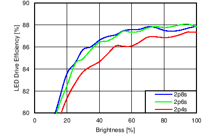
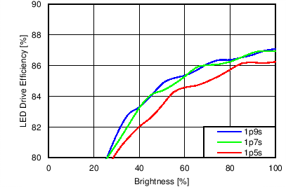
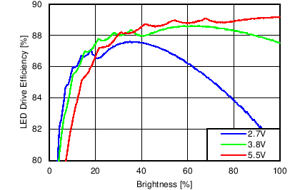
| 6p6s Load |
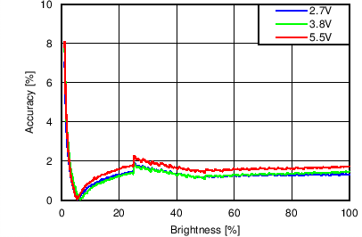
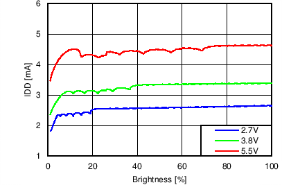
Function of VDD
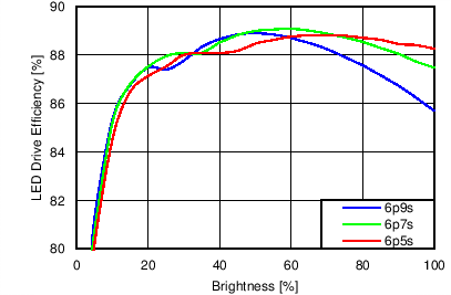
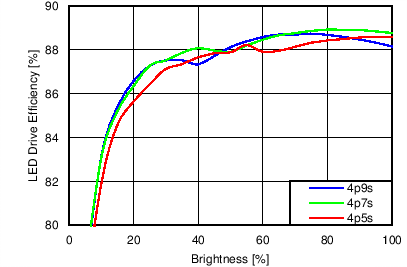
| 6p6s Load |
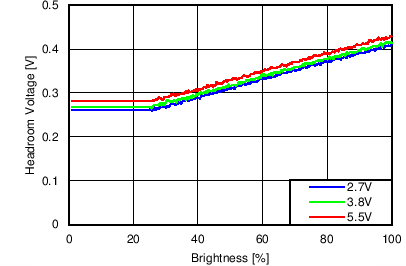
Function of VDD
