SNVSA71 February 2015 LP8728C-Q1
PRODUCTION DATA.
- 1 Features
- 2 Applications
- 3 Description
- 4 Revision History
- 5 Pin Configuration and Functions
- 6 Specifications
- 7 Detailed Description
- 8 Application and Implementation
- 9 Power Supply Recommendations
- 10Layout
- 11Device and Documentation Support
- 12Mechanical, Packaging, and Orderable Information
パッケージ・オプション
メカニカル・データ(パッケージ|ピン)
- RSG|28
サーマルパッド・メカニカル・データ
- RSG|28
発注情報
8 Application and Implementation
NOTE
Information in the following applications sections is not part of the TI component specification, and TI does not warrant its accuracy or completeness. TI’s customers are responsible for determining suitability of components for their purposes. Customers should validate and test their design implementation to confirm system functionality.
8.1 Application Information
The LP8728C-Q1 is a quad-output Power Management Unit (PMU), optimized for low-power FPGAs, microprocessors, and DSPs.
8.2 Typical Application
Figure 15 shows an example of a typical application. A microcontroller controls each buck converter with separate enable signals. All four power good signals are connected to a microcontroller with dedicated pullup resistors. If only one master power good signal is required all power good signals can be connected in parallel and pulled up with a single pullup resistor. VOUT3 output voltage can be selected with a DEFSEL input. If VOUT3 output voltage control is not required during operation, output voltage can be selected by connecting DEFSEL pin to VDDIO or to GND.
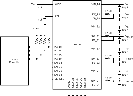 Figure 15. LP8728C-Q1 Typical Application Schematic
8.2.1 Design Requirements
| DESIGN PARAMETER | EXAMPLE VALUE |
|---|---|
| Input voltage range (VIN) | 4.5 V to 5.5 V |
| Buck converter output current | 1 A maximum |
| Buck converter input capacitance | 10 µF, 6.3 V |
| Buck converter output capacitance | 10 µF, 6.3 V |
| Buck converter inductor | 1.5 µH, 1.5 A |
| AVDD pin bypass capacitor | 1 µF, 6.3 V |
| BYP pin bypass capacitor | 1 µF, 6.3 V |
8.2.2 Detailed Design Procedure
8.2.2.1 Inductor
The four converters operate with 1.5-µH inductors. The inductor has to be selected based on the DC resistance and saturation current. The DC resistance of the inductor directly effects the efficiency of the converter. Therefore, an inductor with the lowest possible DC resistance should be selected for good efficiency. The inductor should have a saturation current rating equal or higher than the high-side switch current limit (1500 mA). To minimize radiated noise shielded inductor should be used. The inductor should be placed as close to the LP8728C-Q1 as possible, and the trace from the inductor to the buck converter switch pin needs to be wide enough to withstand the high switching currents.
8.2.2.2 Input and Output Capacitors
Because buck converters have a discontinuous input current, a low equivalent series resistance (ESR) input capacitor is required for the best input-voltage filtering and to minimize interference with other circuits caused by high input voltage spikes. Each DC-DC converter requires a 10-µF ceramic input capacitor on its input pin VIN_Bx. The input capacitor capacitance can be increased without any limit for better input voltage filtering. Voltage rating of the capacitors should be at least 10V. A small 100-nF capacitor can be used in parallel to minimize high-frequency interferences. Input capacitors should be placed as close to the VIN_Bx pins as possible. Routing from input capacitor to VIN_Bx pins should be done on top layer without using any vias.
An output capacitor with a typical value of 10 µF is recommended for each converter. Ceramic capacitors with low ESR value have lowest output voltage ripple and are recommended.
Some ceramic capacitors, especially those in small packages, exhibit a strong capacitance reduction with the increased applied DC voltage (DC bias effect). The capacitance value can fall below half of the nominal capacitance. This needs to be taken into consideration and, if necessary, use a capacitor with higher value or higher voltage rating.
Table 1. Recommended External Components
| COMPONENT | DESCRIPTION | VALUE | TYPE | EXAMPLE |
|---|---|---|---|---|
| CIN_B1,2,3,4 | Buck regulator input capacitor | 10 µF | Ceramic, 10 V, X7R | MuRata, GRM21BR71A106KE51L |
| COUT_B1,2,3,4 | Buck regulator output capacitor | 10 µF | Ceramic, 10 V, X7R | MuRata, GRM21BR71A106KE51L |
| CAVDD | AVDD pin input capacitor | 1 µF | Ceramic, 10 V, X7R | MuRata, GRM188R71A105KA61D |
| CBYP | Internal LDO bypass capacitor | 1 µF | Ceramic, 10 V, X7R | MuRata, GRM188R71A105KA61D |
| LSW1,2,3 4 | Buck regulator inductor | 1.5 µH | ISAT >1.5 A, DCR < 100 mΩ | TOKO MDT2520-CN1R5M |
8.2.3 Application Performance Plots
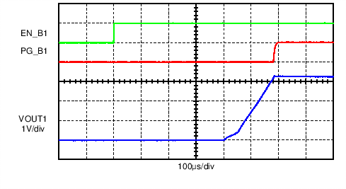
Unless otherwise noted, VIN = 5 V, TA = 25°C, inductor type: TOKO MDT2520-CN1R5M, input and output capacitor type: MuRata GRM21BR71A106KE51L.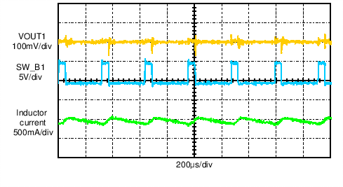
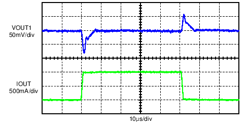
| IOUT from 0 mA to 1A, tRISE = tFALL = 1 µs | ||
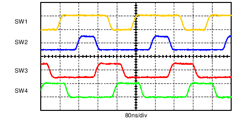
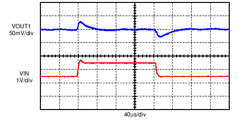
| VIN from 4.5 V To 5.5 V, tRISE = tFALL = 10 µs | ||