SNVSA28 December 2014 LP8731-Q1
PRODUCTION DATA.
- 1 Features
- 2 Applications
- 3 Description
- 4 Revision History
- 5 Device Comparison Tables
- 6 Pin Configuration and Functions
-
7 Specifications
- 7.1 Absolute Maximum Ratings
- 7.2 ESD Ratings
- 7.3 Recommended Operating Conditions (Bucks)
- 7.4 Thermal Information
- 7.5 General Electrical Characteristics
- 7.6 Low Dropout Regulators, LDO1 And LDO2
- 7.7 Buck Converters SW1, SW2
- 7.8 I/O Electrical Characteristics
- 7.9 Power-On Reset Threshold/Function (POR)
- 7.10 I2C-Compatible Interface Timing
- 7.11 Typical Characteristics
-
8 Detailed Description
- 8.1 Overview
- 8.2 Functional Block Diagram
- 8.3
Features Description
- 8.3.1 Linear Low Dropout Regulators (LDOs)
- 8.3.2 No-Load Stability
- 8.3.3 LDO1 and LDO2 Control Registers
- 8.3.4
SW1, SW2: Synchronous Step-Down Magnetic DC-DC Converters
- 8.3.4.1 Functional Description
- 8.3.4.2 Circuit Operation
- 8.3.4.3 PWM Operation
- 8.3.4.4 Internal Synchronous Rectification
- 8.3.4.5 Current Limiting
- 8.3.4.6 SW1, SW2 Operation
- 8.3.4.7 SW1, SW2 Control Registers
- 8.3.4.8 Shutdown Mode
- 8.3.4.9 Soft Start
- 8.3.4.10 Low Dropout Operation
- 8.3.4.11 Flexible Power Sequencing of Multiple Power Supplies
- 8.3.4.12 Power-Up Sequencing Using the EN_T Function
- 8.3.5 Flexible Power-On Reset (for example, Power Good with Delay)
- 8.3.6 Undervoltage Lockout
- 8.4 Device Functional Modes
- 8.5 Programming
- 8.6
LP8731-Q1 Register Maps
- 8.6.1 Interrupt Status Register (ISRA) 0x02
- 8.6.2 System Control 1 Register (SCR1) 0x07
- 8.6.3 EN_DLY Preset Delay Sequence after EN_T Assertion
- 8.6.4 Buck and LDO Output Voltage Enable Register (BKLDOEN) - 0x10
- 8.6.5 Buck and LDO Status Register (BKLDOSR) - 0x11
- 8.6.6 BUCK Voltage Change Control Register 1 (VCCR) - 0x20
- 8.6.7 BUCK1 Target Voltage 1 Register (B1TV1) - 0x23
- 8.6.8 BUCK1 Target Voltage 2 Register (B1TV2) - 0x24
- 8.6.9 BUCK1 Ramp Control Register (B1RC) - 0x25
- 8.6.10 BUCK2 Target 1 Register (B2TV1) - 0x29
- 8.6.11 BUCK2 Target 2 Register (B2TV2) - 0x2A
- 8.6.12 BUCK2 Ramp Control Register (B2RC) - 0x2B
- 8.6.13 BUCK Function Register (BFCR) - 0x38
- 8.6.14 Spread Spectrum Function
- 8.6.15 LDO1 Control Register (LDO1VCR) - 0x39
- 8.6.16 LDO2 Control Register (LDO2VCR) - 0x3A
- 9 Application and Implementation
- 10Power Supply Recommendations
- 11Layout
- 12Device and Documentation Support
- 13Mechanical, Packaging, and Orderable Information
7 Specifications
7.1 Absolute Maximum Ratings
over operating free-air temperature range (unless otherwise noted)(1)| MIN | MAX | UNIT | ||
|---|---|---|---|---|
| VIN, SDA, SCL | −0.3 | 6 | V | |
| GND to GND SLUG | ±0.3 | |||
| Power dissipation (PD_MAX) | Internally limited | |||
| Junction temperature (TJ-MAX) | 150 | °C | ||
| Maximum lead temperature (soldering) | 260 | |||
| Storage temperature (Tstg ) | –65 | 150 | ||
(1) Stresses beyond those listed under absolute maximum ratings may cause permanent damage to the device. These are stress ratings only, and functional operation of the device at these or any other conditions beyond those indicated under recommended operating conditions is not implied. Exposure to absolute–maximum–rated conditions for extended periods may affect device reliability.
7.2 ESD Ratings
| VALUE | UNIT | |||
|---|---|---|---|---|
| V(ESD) | Electrostatic discharge | Human-body model (HBM), per AEC Q100-002(1) | ±2000 | V |
| Charged-device model (CDM), per AEC Q100-011 | ±750 | |||
(1) AEC Q100-002 indicates that HBM stressing shall be in accordance with the ANSI/ESDA/JEDEC JS-001 specification.
7.3 Recommended Operating Conditions (Bucks)
over operating free-air temperature range (unless otherwise noted)| MIN | MAX | UNIT | ||
|---|---|---|---|---|
| VIN | 2.8 | 5.5 | V | |
| VEN | 0 | (VIN + 0.3) | ||
| Junction temperature (TJ) | –40 | 125 | °C | |
| Ambient temperature (TA) | –40 | 125 | ||
7.4 Thermal Information
| THERMAL METRIC(1) | LP8731-Q1 | UNIT | |
|---|---|---|---|
| DSBGA (YZR) | |||
| 25 PINS | |||
| RθJA | Junction-to-ambient thermal resistance | 58.7 | °C/W |
| RθJC(top) | Junction-to-case (top) thermal resistance | 0.3 | |
| RθJB | Junction-to-board thermal resistance | 8 | |
| ψJT | Junction-to-top characterization parameter | 0.6 | |
| ψJB | Junction-to-board characterization parameter | 8 | |
| RθJC(bot) | Junction-to-case (bottom) thermal resistance | n/a | |
(1) For more information about traditional and new thermal metrics, see the IC Package Thermal Metrics application report, SPRA953.
7.5 General Electrical Characteristics
Unless otherwise noted, VIN = 3.6 V. Typical values and limits apply for TJ = 25°C.(1)| PARAMETER | TEST CONDITIONS | MIN | TYP | MAX | UNIT | |
|---|---|---|---|---|---|---|
| IQ | VINLDO12 shutdown current | VIN = 3.6 V | 3 | µA | ||
| VPOR | Power-on reset threshold | VDD Falling Edge(2) | 1.9 | V | ||
| TSD | Thermal shutdown threshold | 160 | °C | |||
| TSDH | Thermal shutdown hysteresis | 20 | ||||
| UVLO | Undervoltage lockout | Rising | 2.9 | V | ||
| Falling | 2.7 | |||||
(1) All voltages are with respect to the potential at the GND pin.
(2) VPOR is voltage at which the EPROM resets. This is different from the UVLO on VINLDO12, which is the voltage at which the regulators shut off; and is also different from the nPOR function, which signals if the regulators are in a specified range.
7.6 Low Dropout Regulators, LDO1 And LDO2
Unless otherwise noted, VIN = 3.6 V, CIN = 1 µF, COUT = 0.47 µF. Typical values and limits apply for TJ = 25°C.(1)(2)(3)| PARAMETER | TEST CONDITIONS | MIN | TYP | MAX | UNIT | |
|---|---|---|---|---|---|---|
| VIN | Operational voltage range | VINLDO1 and VINLDO2 PMOS pins(4) | 2.45(5) | 5.5(5) | V | |
| VOUT Accuracy | Output voltage accuracy (default VOUT) | Load current = 1 mA | −3%(5) | 3%(5) | ||
| ΔVOUT | Line regulation | VIN = (VOUT + 0.3 V) to 5 V(6)
Load current = 1 mA |
0.2(5) | %/V | ||
| Load regulation | VIN = 3.6 V, Load current = 1 mA to IMAX |
0.011(5) | %/mA | |||
| ISC | Short circuit current limit | LDO1 to LDO2, VOUT = 0 V | 500 | mA | ||
| VIN – VOUT | Dropout voltage | Load current = 50 mA at VOUT = 2.8 V(7) | 30 | 50(5) | mV | |
| Load current = 250 mA at VOUT = 2.8 V | 150 | 200(5) | ||||
| PSRR | Power supply ripple rejection | ƒ = 10 kHz, Load current = IMAX | 45 | dB | ||
| θn | Supply output noise | 10 Hz < F < 100 KHz | 280 | µVrms | ||
| IQ(8)(9) | Quiescent current “on” | IOUT = 0 mA | 40 | µA | ||
| Quiescent current “on” | IOUT = IMAX | 60 | µA | |||
| Quiescent current “off” | EN is de-asserted(10) | 0.03 | µA | |||
| TON | Turn-on time | Start-up from shutdown | 300 | µs | ||
| COUT | Output capacitance | Capacitance for stability 0°C ≤ TJ ≤ 125°C | 0.33 | 0.47 | µF | |
| −40°C ≤ TJ ≤ 125°C | 0.68 | 1 | µF | |||
| ESR | 5 | 500 | mΩ | |||
(1) All voltages are with respect to the potential at the GND pin.
(2) Minimum and Maximum limits are ensured by design, test, or statistical analysis. Typical numbers are not ensured, but do represent the most likely norm.
(3) CIN, COUT: Low-ESR Surface-Mount Ceramic Capacitors (MLCCs) used in setting electrical characteristics.
(4) Pins A1 and/or A5 can operate from VIN min of 1.74 to a VIN max of 5.5 V. This rating is only for the series pass PMOS power FET. It allows the system design to use a lower voltage rating if the input voltage comes from a buck output. However, if VIN is required to operate at a higher voltage than other device supply pins, it is necessary to wire the VINLDO12 pins (B4 an B5) and VINLDO1 and VINLDO2 pins (A1 and/or A5) together to that higher voltage so that the LDO core supply has sufficient head-room to operate the gate of the PMOS.
(5) Limits apply over the entire operating junction temperature range for operation, –40°C to 125°C.
(6) VIN minimum for line regulation values is 1.8 V.
(7) Dropout voltage is the voltage difference between the input and the output at which the output voltage drops to 100 mV below its nominal value.
(8) Quiescent current is defined here as the difference in current between the input voltage source and the load at VOUT.
(9) The IQ can be defined as the standing current of the LP8731-Q1 when the I2C bus is activated and all other power blocks have been disabled via the I2C bus, or it can be defined as the I2C bus active, and the other power blocks are active under no load condition. These two values can be used by the system designer when the LP8731-Q1 is powered using a battery.
(10) The IQ exhibits a higher current draw when the EN pin is de-asserted because the I2C buffer pins draw an additional 2 µA.
7.7 Buck Converters SW1, SW2
Unless otherwise noted, VIN = 3.6 V, CIN = 10 µF, COUT = 10 µF, LOUT = 2.2 µH ceramic. Typical values and limits apply for TJ = 25°C.(1)(2)(3)| PARAMETER | TEST CONDITIONS | MIN | TYP | MAX | UNIT | |
|---|---|---|---|---|---|---|
| VFB | Feedback voltage | −3%(4) | 3%(4) | |||
| VOUT | Line regulation | 2.8 V < VIN < 5.5 V IOUT = 10 mA |
0.089% | /V | ||
| Load regulation | 100 mA < IO < IMAX | 0.0013% | /mA | |||
| Output accuracy(5) | VIN = 3.3 V, VOUT from 0.8875 V to 1.1625 V Load from 0 mA to 600 mA |
–2%(4) | 2%(4) | |||
| Eff | Efficiency | Load current = 250 mA | 90% | |||
| ISHDN | Shutdown supply current | EN is de-asserted | 0.01 | µA | ||
| fOSC | Internal oscillator frequency | 1.7(4) | 2.1 | MHz | ||
| IPEAK | Buck1 peak switching current limit | 1.7 | A | |||
| Buck2 peak switching current limit | 1.7 | |||||
| IQ(6) | Quiescent current “on” | No load PWM Mode | 2 | mA | ||
| RDSON (P) | Pin-pin resistance PFET | 200 | mΩ | |||
| RDSON (N) | Pin-pin resistance NFET | 180 | mΩ | |||
| TON | Turn-on time | Start-up from shutdown | 500 | µs | ||
| CIN | Input capacitance | Capacitance for stability | 10 | µF | ||
| CO | Output capacitance | Capacitance for stability | 10 | µF | ||
(1) All voltages are with respect to the potential at the GND pin.
(2) Minimum and Maximum limits are ensured by design, test, or statistical analysis. Typical numbers are not ensured, but do represent the most likely norm.
(3) CIN, COUT: Low-ESR Surface-Mount Ceramic Capacitors (MLCCs) used in setting electrical characteristics.
(4) Limits apply over the entire operating junction temperature range for operation, –40°C to 125°C
(5) Based on closed loop, bench test data with LP8731YZREVM.
(6) The IQ can be defined as the standing current of the LP8731-Q1 when the I2C bus is active and all other power blocks have been disabled via the I2C bus, or it can be defined as the I2C bus active, and the other power blocks are active under no load condition. These two values can be used by the system designer when the LP8731-Q1 is powered using a battery.
7.8 I/O Electrical Characteristics
| PARAMETER | TEST CONDITIONS | MIN | TYP | MAX | UNIT | |
|---|---|---|---|---|---|---|
| VIL | Input low level | 0.4(1) | V | |||
| VIH | Input high level | 1.2(1) | ||||
(1) This specification is ensured by design.
7.9 Power-On Reset Threshold/Function (POR)
| PARAMETER | TEST CONDITIONS | MIN | TYP | MAX | UNIT | |
|---|---|---|---|---|---|---|
| nPOR | nPOR = Power-on reset for Buck1 and Buck2 | Default | 50 | µs | ||
| nPOR threshold | Percentage of target voltage Buck1 or Buck2 | VBUCK1 AND VBUCK2 rising | 94% | |||
| VBUCK1 OR VBUCK2 falling | 85% | |||||
| VOL | Output level low | Load = IOL = 0.2 mA | 0.23 | 0.5(1) | V | |
(1) This specification is ensured by design.
7.10 I2C-Compatible Interface Timing
Unless otherwise noted, VIN = 3.6 V. Nominal values and limits apply for TJ = 25°C.(1)| MIN | NOM | MAX | UNIT | |||
|---|---|---|---|---|---|---|
| ƒCLK | Clock frequency | 400 | kHz | |||
| tBF | Bus-free time between start and stop | See(1) | 1.3 | µs | ||
| tHOLD | Hold time repeated start condition | See(1) | 0.6 | µs | ||
| tCLKLP | CLK low period | See(1) | 1.3 | µs | ||
| tCLKHP | CLK high period | See(1) | 0.6 | µs | ||
| tSU | Setup time repeated start condition | See(1) | 0.6 | µs | ||
| tDATAHLD | Data hold time | See(1) | 0 | µs | ||
| tDATASU | Data setup time | See(1) | 100 | ns | ||
| TSU | Setup time for start condition | See(1) | 0.6 | µs | ||
| TTRANS | Maximum pulse width of spikes that must be suppressed by the input filter of both DATA & CLK signals | See(1) | 50 | ns | ||
(1) This specification is ensured by design.
7.11 Typical Characteristics
TA = 25°C unless otherwise noted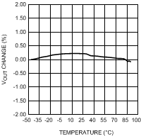
| VIN = 3.6 V | VOUT = 2.6 V | 100-mA load |
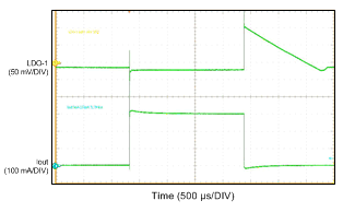
| VOUT = 3.6 V | ILOAD = 0 to 300 mA | |
| VOUT = 1.8 V | Tr = Tf = 1 µs | |
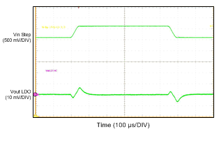
| VIN = 3.6 V to 4.2 V | ILOAD = 300 mA | |
| VOUT = 1.8 V | Tr = Tf = 20 µs | |
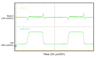
| IOUT = 200 mA to 1.2 A PWM | ||
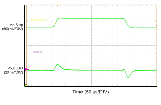
| VIN Step | IOUT = 1.2 A | Tr = Tf = 10 µs |
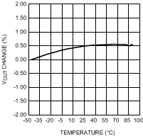
| VIN = 3.6 V | VOUT = 3.3 V | 100-mA load |
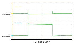
| VOUT = 3.6 V | ILOAD = 0 to 300 mA | |
| VOUT = 1.8 V | Tr = Tf = 4 µs | |
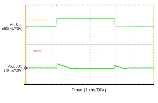
| VIN = 3.6 V to 4.2 V | IOUT = 1 mA | |
| VOUT = 1.8 V | Tr = Tf = 30 µs | |
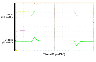
| VIN Step | IOUT = 300 mA | Tr = Tf = 30 µs |
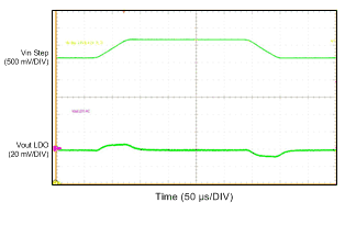
| VIN Step | IOUT = 1.2 A | Tr = Tf = 30 µs |