JAJSG84B January   2016  – June 2018 LP8758-E0

PRODUCTION DATA.  

  1. 特長
  2. アプリケーション
  3. 概要
    1.     Device Images
      1.      概略回路図
      2.      効率と出力電流との関係
  4. 改訂履歴
  5. Pin Configuration and Functions
    1.     Pin Functions
  6. Specifications
    1. 6.1 Absolute Maximum Ratings
    2. 6.2 ESD Ratings
    3. 6.3 Recommended Operating Conditions
    4. 6.4 Thermal Information
    5. 6.5 Electrical Characteristics
    6. 6.6 I2C Serial Bus Timing Requirements
    7. 6.7 Switching Characteristics
    8. 6.8 Typical Characteristics
  7. Detailed Description
    1. 7.1 Overview
      1. 7.1.1 Buck Information
        1. 7.1.1.1 Operating Modes
        2. 7.1.1.2 Programmability
        3. 7.1.1.3 Features
    2. 7.2 Functional Block Diagram
    3. 7.3 Feature Description
      1. 7.3.1 Overview
        1. 7.3.1.1 Transition between PWM and PFM Modes
        2. 7.3.1.2 Buck Converter Load Current Measurement
        3. 7.3.1.3 Spread-Spectrum Mode
      2. 7.3.2 Power-Up
      3. 7.3.3 Regulator Control
        1. 7.3.3.1 Enabling and Disabling
        2. 7.3.3.2 Changing Output Voltage
      4. 7.3.4 Device Reset Scenarios
      5. 7.3.5 Diagnosis and Protection Features
        1. 7.3.5.1 Warnings for Diagnosis (Interrupt)
          1. 7.3.5.1.1 Output Current Limit
          2. 7.3.5.1.2 Thermal Warning
        2. 7.3.5.2 Protection (Regulator Disable)
          1. 7.3.5.2.1 Short-Circuit and Overload Protection
          2. 7.3.5.2.2 Thermal Shutdown
        3. 7.3.5.3 Fault (Power Down)
          1. 7.3.5.3.1 Undervoltage Lockout
      6. 7.3.6 Digital Signal Filtering
    4. 7.4 Device Functional Modes
      1. 7.4.1 Modes of Operation
    5. 7.5 Programming
      1. 7.5.1 I2C-Compatible Interface
        1. 7.5.1.1 Data Validity
        2. 7.5.1.2 Start and Stop Conditions
        3. 7.5.1.3 Transferring Data
        4. 7.5.1.4 I2C-Compatible Chip Address
        5. 7.5.1.5 Auto Increment Feature
    6. 7.6 Register Maps
      1. 7.6.1 Register Descriptions
        1. 7.6.1.1  OTP_REV
        2. 7.6.1.2  BUCK0_CTRL1
        3. 7.6.1.3  BUCK0_CTRL2
        4. 7.6.1.4  BUCK1_CTRL1
        5. 7.6.1.5  BUCK1_CTRL2
        6. 7.6.1.6  BUCK2_CTRL1
        7. 7.6.1.7  BUCK2_CTRL2
        8. 7.6.1.8  BUCK3_CTRL1
        9. 7.6.1.9  BUCK3_CTRL2
        10. 7.6.1.10 BUCK0_VOUT
        11. 7.6.1.11 BUCK0_FLOOR_VOUT
        12. 7.6.1.12 BUCK1_VOUT
        13. 7.6.1.13 BUCK1_FLOOR_VOUT
        14. 7.6.1.14 BUCK2_VOUT
        15. 7.6.1.15 BUCK2_FLOOR_VOUT
        16. 7.6.1.16 BUCK3_VOUT
        17. 7.6.1.17 BUCK3_FLOOR_VOUT
        18. 7.6.1.18 BUCK0_DELAY
        19. 7.6.1.19 BUCK1_DELAY
        20. 7.6.1.20 BUCK2_DELAY
        21. 7.6.1.21 BUCK3_DELAY
        22. 7.6.1.22 RESET
        23. 7.6.1.23 CONFIG
        24. 7.6.1.24 INT_TOP
        25. 7.6.1.25 INT_BUCK_0_1
        26. 7.6.1.26 INT_BUCK_2_3
        27. 7.6.1.27 TOP_STAT
        28. 7.6.1.28 BUCK_0_1_STAT
        29. 7.6.1.29 BUCK_2_3_STAT
        30. 7.6.1.30 TOP_MASK
        31. 7.6.1.31 BUCK_0_1_MASK
        32. 7.6.1.32 BUCK_2_3_MASK
        33. 7.6.1.33 SEL_I_LOAD
        34. 7.6.1.34 I_LOAD_2
        35. 7.6.1.35 I_LOAD_1
  8. Application and Implementation
    1. 8.1 Application Information
    2. 8.2 Typical Application
      1. 8.2.1 Design Requirements
      2. 8.2.2 Detailed Design Procedure
        1. 8.2.2.1 Application Components
          1. 8.2.2.1.1 Inductor Selection
          2. 8.2.2.1.2 Input Capacitor Selection
          3. 8.2.2.1.3 Output Capacitor Selection
      3. 8.2.3 Application Curves
  9. Power Supply Recommendations
  10. 10Layout
    1. 10.1 Layout Guidelines
    2. 10.2 Layout Example
  11. 11デバイスおよびドキュメントのサポート
    1. 11.1 デバイス・サポート
      1. 11.1.1 デベロッパー・ネットワークの製品に関する免責事項
    2. 11.2 ドキュメントのサポート
      1. 11.2.1 関連資料
    3. 11.3 ドキュメントの更新通知を受け取る方法
    4. 11.4 コミュニティ・リソース
    5. 11.5 商標
    6. 11.6 静電気放電に関する注意事項
    7. 11.7 Glossary
  12. 12メカニカル、パッケージ、および注文情報

パッケージ・オプション

メカニカル・データ(パッケージ|ピン)
サーマルパッド・メカニカル・データ
発注情報

Output Current Limit

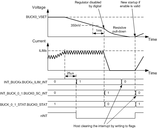
The converter cores have programmable output peak current limits. The limits are individually programmed for all buck converter cores with BUCKx_CTRL2.ILIMx[2:0] bits. If the load current is increased so that the current limit is triggered, the regulator continues to regulate to the limit current level (current peak regulation). The voltage may decrease if the load current is higher than limit current. If the current regulation continues for 20 µs, the LP8758-E0 device sets the INT_BUCKx.BUCKx_ILIM_INT bit and pulls the nINT pin low. The host processor can read BUCKx_STAT.BUCKx_ILIM_STAT bits to see if the converter cores is still in peak current regulation mode.

For example, if the load on Buck0 output is so high that the output voltage VOUT decreases below a 350-mV level, the LP8758-E0 device disables the converter core Buck0 and sets the INT_BUCK_0_1.BUCK0_SC_INT bit. In addition the BUCK_0_1_STAT.BUCK0_STAT bit is set to 0. The interrupt is cleared when the host processor writes 1 to INT_BUCK_0_1.BUCK0_SC_INT bit. The overload situation is shown in Figure 11.
LP8758-E0 Overload_4ph.gifFigure 11. Overload Situation