JAJSQQ8A July 2023 – November 2023 LP8868U-Q1 , LP8868V-Q1 , LP8868W-Q1 , LP8868X-Q1 , LP8868Y-Q1 , LP8868Z-Q1
PRODUCTION DATA
- 1
- 1 特長
- 2 アプリケーション
- 3 概要
- 4 Comparison Table
- 5 Pin Configuration and Functions
- 6 Specifications
- 7 Detailed Description
-
8 Application and Implementation
- 8.1 Application Information
- 8.2 Typical Application
- 8.3 Power Supply Recommendations
- 8.4 Layout
- 9 Device and Documentation Support
- 10Revision History
- 11Mechanical, Packaging, and Orderable Information
パッケージ・オプション
メカニカル・データ(パッケージ|ピン)
- DMT|14
サーマルパッド・メカニカル・データ
- DMT|14
発注情報
5 Pin Configuration and Functions
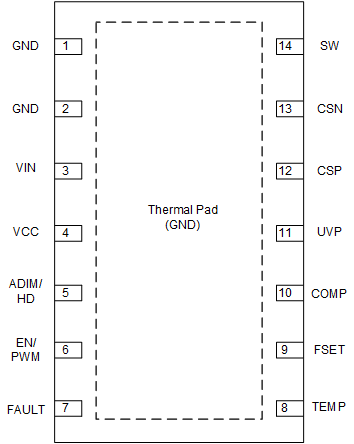
 Figure 5-1 14-Pin Buck
VSONTop View
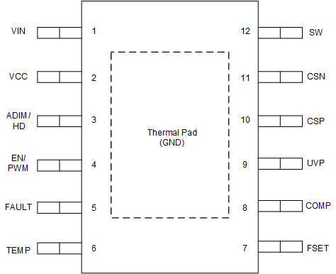
HVSSOP is product preview
Figure 5-2 12-Pin Buck HVSSOPTop ViewTable 5-1 Pin Functions
| PIN | TYPE(1) | DESCRIPTION | |
|---|---|---|---|
| No. | NAME | ||
| 1 | PGND | G | Power ground pin. |
| 2 | AGND | G | Analog ground pin. |
| 3 | VIN | P | Input power pin. |
| 4 | VCC | P | Internal LDO output pin. Connect with a 10-V, 1-uF capacitor to GND. |
| 5 | ADIM/HD | I | Analog dimming or hybrid dimming pin. Pull high for PWM dimming only, pull low for hybrid dimming, input PWM signal for analog dimming. |
| 6 | PWM/EN | I | PWM dimming or EN pin. Pull high for always on, pull low for disabling the device, input PWM signal for PWM dimming. |
| 7 | FAULT | O | Open drain output. Pull low when fault is detected. |
| 8 | TEMP | I/O | Thermal foldback pin. Put different resistor values to GND to set different thermal foldback behavior curves. |
| 9 | FSET | I/O | Switching frequency set pin, with range of 100 kHz ~ 2.2 MHz. Put different resistor values to GND for different switching frequencies. |
| 10 | COMP | I/O | Error-amilifier output. Connect capacitors to GND. Different capacitor values determine different softstart times and bandwidths. |
| 11 | UVP | I | Undervoltage detection pin. Put different resistor dividers to set the LED open detection thresholds. |
| 12 | CSP | I | LED current sense positive pin. |
| 13 | CSN | I | LED current sense negative pin. |
| 14 | SW | P | Switching node pin. Internally connected to the low-side MOSFET. Connect with the power inductor and the schottky diode. |
| Pad | Thermal Pad | G | Power ground pin. |
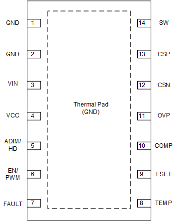
 Figure 5-3 14-Pin
Boost/Buck-Boost VSONTop View
HVSSOP is product preview
Figure 5-4 12-Pin Boost/Buck-Boost HVSSOPTop ViewTable 5-2 Pin Functions for
boost/buck-boost topology
| PIN | TYPE(1) | DESCRIPTION | |
|---|---|---|---|
| VSON Package | NAME | ||
| 1 | PGND | G | Power ground pin. |
| 2 | AGND | G | Analog ground pin. |
| 3 | VIN | P | Input power pin. |
| 4 | VCC | P | Internal LDO output pin. Connect with a 10-V, 1-uF capacitor to GND. |
| 5 | ADIM/HD | I | Analog dimming or hybrid dimming pin. Pull high for PWM dimming only, pull low for hybrid dimming, input PWM signal for analog dimming. |
| 6 | PWM/EN | I | PWM dimming or EN pin. Pull high for always on, pull low for disabling the device, input PWM signal for PWM dimming. |
| 7 | FAULT | O | Open drain output. Pull low when fault is detected. |
| 8 | TEMP | I/O | Thermal foldback pin. Put different resistor values to GND to set different thermal foldback behavior curves. |
| 9 | FSET | I/O | Switching frequency set pin, with range of 100 kHz ~ 2.2 MHz. Put different resistor values to GND for different switching frequencies. |
| 10 | COMP | I/O | Error-amilifier output. Connect capacitors to GND. Different capacitor values determine different softstart times and bandwidths. |
| 11 | OVP | I | Overvoltage detection pin. Put different resistor dividers to set the LED open detection thresholds. |
| 12 | CSN | I | LED current sense negative pin. |
| 13 | CSP | I | LED current sense positive pin. |
| 14 | SW | P | Switching node pin. Internally connected to the low-side MOSFET. Connect with the power inductor and the schottky diode. |
| Pad | Thermal Pad | G | Power ground pin. |
(1) I = Input, O = Output, P = Supply, G = Ground