SNVS542E May 2008 – June 2016 LP8900
PRODUCTION DATA.
- 1 Features
- 2 Applications
- 3 Description
- 4 Revision History
- 5 Default Device Options
- 6 Pin Configuration and Functions
- 7 Specifications
- 8 Detailed Description
- 9 Application and Implementation
- 10Power Supply Recommendations
- 11Layout
- 12Device and Documentation Support
- 13Mechanical, Packaging, and Orderable Information
8 Detailed Description
8.1 Overview
The LP8900 is a dual linear regulator capable of supplying 200 mA output current per regulator. Designed to meet the requirements of RF and analog circuits, the LP8900 provides low device noise, high PSRR, low quiescent current, and superior line transient response figures.
Using new innovative design techniques the LP8900 offers class-leading device noise performance without a noise bypass capacitor. The LP8900 is designed to perform with a single 1-µF input capacitor and a single 1-µF ceramic output capacitor.
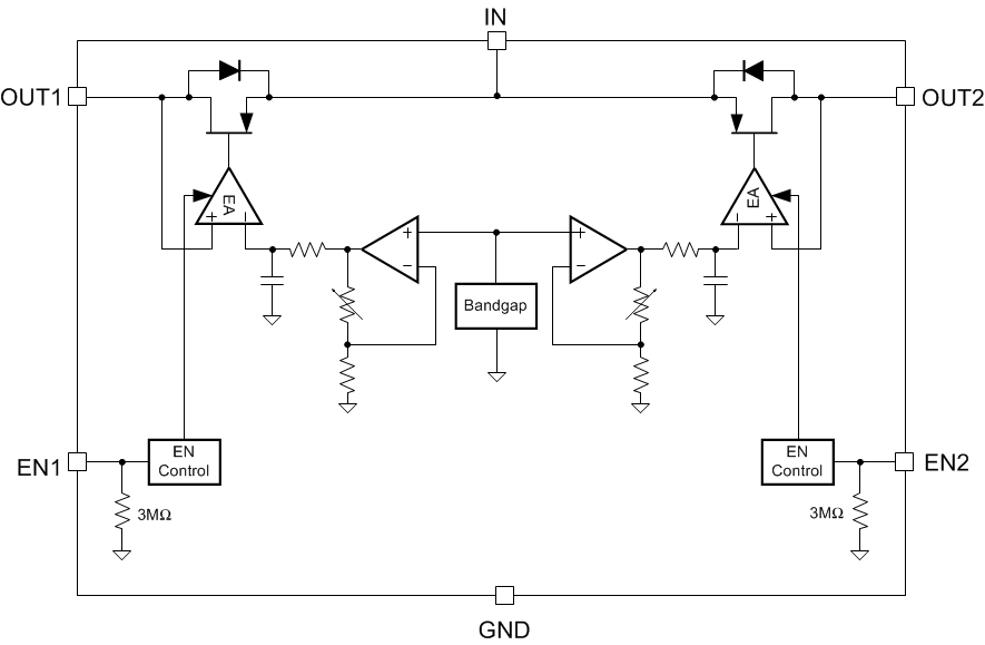
8.2 Functional Block Diagram

8.3 Feature Description
8.3.1 Enable Control
The LP8900 may be switched ON or OFF by a logic input at the EN pin. A high voltage at this pin turns the device on. When the enable pin is low, the regulator output is off and the device typically consumes 3 nA. However if the application does not require the shutdown feature, the EN pin can be tied to VIN to keep the regulator permanently on. To ensure fast start-up is achieved, EN must be driven separately.
A 3-MΩ pulldown resister ties the EN input to ground, this ensures that the device remains off when the enable pin is left open circuit. To ensure proper operation, the signal source used to drive the EN input must be able to swing above and below the specified turnon or turnoff voltage thresholds listed in Electrical Characteristics under VIL and VIH.
8.4 Device Functional Modes
8.4.1 Enable (EN)
The LP8900 EN pin is internally held low by a 3-MΩ resistor to GND. The Enable pin voltage must be higher than the VIH threshold to ensure that the device is fully enabled under all operating conditions.
When the EN pin is pulled low, the output is off and the device typically consumes 3 nA.
8.4.2 Minimum Operating Input Voltage (VIN)
The LP8900 does not include any dedicated UVLO circuitry. The LP8900 internal circuitry is not fully functional until VIN is at least 1.8 V. The output voltage is not regulated until VIN has reached at least the greater of 1.8 V or (VOUT + VDO).