JAJS630E August 2000 – November 2016 LPV321-N , LPV324-N , LPV358-N
PRODUCTION DATA.
- 1 特長
- 2 アプリケーション
- 3 概要
- 4 改訂履歴
- 5 Pin Configuration and Functions
- 6 Specifications
- 7 Detailed Description
- 8 Application and Implementation
- 9 Power Supply Recommendations
- 10Layout
- 11デバイスおよびドキュメントのサポート
- 12メカニカル、パッケージ、および注文情報
パッケージ・オプション
メカニカル・データ(パッケージ|ピン)
サーマルパッド・メカニカル・データ
発注情報
6 Specifications
6.1 Absolute Maximum Ratings
over operating free-air temperature range (unless otherwise noted)(1)| MIN | MAX | UNIT | ||
|---|---|---|---|---|
| Differential input voltage | ±Supply voltage | |||
| Supply voltage (V+– V −) | 5.5 | V | ||
| Output short circuit to V + | See(2) | |||
| Output short circuit to V − | See(3) | |||
| Junction temperature, TJ(MAX)(4) | 150 | °C | ||
| Storage temperature, Tstg | –65 | 150 | °C | |
(1) Stresses beyond those listed under Absolute Maximum Ratings may cause permanent damage to the device. These are stress ratings only, which do not imply functional operation of the device at these or any other conditions beyond those indicated under Recommended Operating Conditions. Exposure to absolute-maximum-rated conditions for extended periods may affect device reliability.
(2) Shorting output to V+ will adversely affect reliability.
(3) Shorting output to V− will adversely affect reliability.
(4) The maximum power dissipation is a function of TJ(MAX) and RθJA. The maximum allowable power dissipation at any ambient temperature is PD = (TJ(MAX) – TA) / RθJA. All numbers apply for packages soldered directly onto a PCB.
6.2 ESD Ratings
| VALUE | UNIT | |||
|---|---|---|---|---|
| LPV321-N in DBV and DCK Packages | ||||
| V(ESD) | Electrostatic discharge | Human-body model (HBM), per ANSI/ESDA/JEDEC JS-001(1) | ±1500 | V |
| Machine model | ±100 | |||
| LPV358-N in D and DGK Packages | ||||
| V(ESD) | Electrostatic discharge | Human-body model (HBM), per ANSI/ESDA/JEDEC JS-001(1) | ±1500 | V |
| Machine model | ±100 | |||
| LPV324-N in D and PW Packages | ||||
| V(ESD) | Electrostatic discharge | Human-body model (HBM), per ANSI/ESDA/JEDEC JS-001(1) | ±2000 | V |
| Machine model | ±100 | |||
(1) Human Body Model, applicable std. MIL-STD-883, Method 3015.7. Machine Model, applicable std. JESD22-A115-A (ESD MM std. of JEDEC)Field-Induced Charge-Device Model, applicable std. JESD22-C101-C (ESD FICDM std. of JEDEC).
6.3 Recommended Operating Conditions
over operating free-air temperature range (unless otherwise noted)| MIN | MAX | UNIT | |
|---|---|---|---|
| Supply voltage | 2.7 | 5 | V |
| Operating temperature | –40 | 85 | °C |
6.4 Thermal Information
| THERMAL METRIC(1) | LPV321-N | LPV358-N | LPV324-N | UNIT | ||||
|---|---|---|---|---|---|---|---|---|
| DBV (SOT-23) |
DCK (SC70) |
DGK (VSSOP) |
D (SOIC) |
D (SOIC) |
PW (TSSOP) |
|||
| 5 PINS | 5 PINS | 8 PINS | 8 PINS | 14 PINS | 14 PINS | |||
| RθJA | Junction-to-ambient thermal resistance | 206.6 | 296.7 | 187.5 | 130.1 | 103.9 | 132.7 | °C/W |
| RθJC(top) | Junction-to-case (top) thermal resistance | 167.2 | 128.1 | 77.7 | 74.3 | 61.6 | 59.1 | °C/W |
| RθJB | Junction-to-board thermal resistance | 65.5 | 74.3 | 108 | 70.7 | 58.4 | 75.1 | °C/W |
| ψJT | Junction-to-top characterization parameter | 50.2 | 6.5 | 15.2 | 23.1 | 21.2 | 10.8 | °C/W |
| ψJB | Junction-to-board characterization parameter | 65.1 | 73.6 | 106.5 | 70.2 | 58.1 | 74.58 | °C/W |
| RθJC(bot) | Junction-to-case (bottom) thermal resistance | — | — | — | — | — | — | °C/W |
(1) For more information about traditional and new thermal metrics, see the Semiconductor and IC Package Thermal Metrics application report.
6.5 DC Electrical Characteristics – 2.7 V
TJ = 25°C, V+ = 2.7 V, V− = 0 V, VCM = 1 V, VO = V+/2, and R L > 1 MΩ (unless otherwise noted)| PARAMETER | TEST CONDITIONS | MIN(1) | TYP(2) | MAX(1) | UNIT | |
|---|---|---|---|---|---|---|
| VOS | Input offset voltage | 1.2 | 7 | mV | ||
| TCVOS | Input offset voltage average drift | 2 | µV/°C | |||
| IB | Input bias current | 1.7 | 50 | nA | ||
| IOS | Input offset current | 0.6 | 40 | nA | ||
| CMRR | Common mode rejection ratio | 0 V ≤ VCM ≤ 1.7 V | 50 | 70 | dB | |
| PSRR | Power supply rejection ratio | 2.7 V ≤ V+ ≤ 5 V, VO = 1 V, VCM = 1 V | 50 | 65 | dB | |
| VCM | Input common-mode voltage | For CMRR ≥ 50 dB | 0 | −0.2 | V | |
| 1.9 | 1.7 | |||||
| VO | Output swing | RL = 100 kΩ to 1.35 V | V+ − 100 | V+ − 3 | mV | |
| 80 | 180 | |||||
| IS | Supply current | LPV321-N | 4 | 8 | µA | |
| LPV358-N, both amplifiers | 8 | 16 | ||||
| LPV324-N, all four amplifiers | 16 | 24 | ||||
(1) All limits are specified by testing or statistical analysis.
(2) Typical values represent the most likely parametric norm as determined at the time of characterization. Actual typical values may vary over time and will also depend on the application and configuration. The typical values are not tested and are not ensured on shipped production material.
6.6 AC Electrical Characteristics – 2.7 V
TJ = 25°C, V+ = 2.7 V, V− = 0 V, VCM = 1 V, VO = V+/2, and R L > 1 MΩ (unless otherwise noted)| PARAMETER | TEST CONDITIONS | MIN(1) | TYP(2) | MAX(1) | UNIT | |
|---|---|---|---|---|---|---|
| GBWP | Gain-bandwidth product | CL = 22 pF | 112 | kHz | ||
| Φm | Phase margin | 97 | ° | |||
| Gm | Gain margin | 35 | dB | |||
| en | Input-referred voltage noise | f = 1 kHz | 178 | nV/√Hz | ||
| in | Input-referred current noise | f = 1 kHz | 0.5 | pA/√Hz | ||
6.7 DC Electrical Characteristics – 5 V
TJ = 25°C, V+ = 5 V, V− = 0 V, VCM = 2 V, VO = V+/2, and R L > 1 MΩ (unless otherwise noted)| PARAMETER | TEST CONDITIONS | MIN(1) | TYP(2) | MAX(1) | UNIT | ||
|---|---|---|---|---|---|---|---|
| VOS | Input offset voltage | TJ = 25°C | 1.5 | 7 | mV | ||
| TJ = –40°C to 85°C | 10 | ||||||
| TCVOS | Input offset voltage average drift | 2 | µV/°C | ||||
| IB | Input bias current | TJ = 25°C | 2 | 50 | nA | ||
| TJ = –40°C to 85°C | 60 | ||||||
| IOS | Input offset current | TJ = 25°C | 0.6 | 40 | nA | ||
| TJ = –40°C to 85°C | 50 | ||||||
| CMRR | Common mode rejection ratio | 0 V ≤ VCM ≤ 4 V | 50 | 71 | dB | ||
| PSRR | Power supply rejection ratio | 2.7 V ≤ V+ ≤ 5 V, VO = 1 V, VCM = 1 V | 50 | 65 | dB | ||
| VCM | Input common-mode voltage | For CMRR ≥ 50 dB | 0 | −0.2 | V | ||
| 4.2 | 4 | ||||||
| AV | Large signal voltage gain(1) | RL = 100 kΩ | TJ = 25°C | 15 | 100 | V/mV | |
| TJ = –40°C to 85°C | 10 | ||||||
| VO | Output swing | Sourcing RL = 100 kΩ to 2.5 V |
TJ = 25°C | V+ −100 | V+ −3.5 | mV | |
| TJ = –40°C to 85°C | V+ −200 | ||||||
| Sinking RL = 100 kΩ to 2.5 V |
TJ = 25°C | 90 | 180 | ||||
| TJ = –40°C to 85°C | 220 | ||||||
| IO | Output short circuit current sourcing | LPV3xx-N, VO = 0 V | 2 | 16 | mA | ||
| Output short circuit current sinking | LPV321-N, VO = 5 V | 20 | 60 | ||||
| LPV324-N and LPV358-N, VO = 5 V | 11 | 16 | |||||
| IS | Supply current | LPV321-N | TJ = 25°C | 9 | 12 | µA | |
| TJ = –40°C to 85°C | 15 | ||||||
| LPV358-N, Both amplifiers |
TJ = 25°C | 15 | 20 | ||||
| TJ = –40°C to 85°C | 24 | ||||||
| LPV324-N, All four amplifiers |
TJ = 25°C | 28 | 42 | ||||
| TJ = –40°C to 85°C | 46 | ||||||
(1) RL is connected to V -. The output voltage is 0.5 V ≤ VO ≤ 4.5 V.
6.8 AC Electrical Characteristics – 5 V
TJ = 25°C, V+ = 5 V, V− = 0 V, VCM = 2 V, VO = V+/2, and R L > 1MΩ (unless otherwise noted)| PARAMETER | TEST CONDITIONS | MIN(1) | TYP(2) | MAX(1) | UNIT | |
|---|---|---|---|---|---|---|
| SR | Slew rate(1) | 0.1 | V/µs | |||
| GBWP | Gain-bandwidth product | CL = 22 pF | 152 | kHz | ||
| Φm | Phase margin | 87 | ° | |||
| Gm | Gain margin | 19 | dB | |||
| en | Input-referred voltage noise | f = 1 kHz | 146 | nV/√Hz | ||
| in | Input-referred current noise | f = 1 kHz | 0.3 | pA/√Hz | ||
(1) Connected as voltage follower with 3V step input. Number specified is the slower of the positive and negative slew rates.
6.9 Typical Characteristics
VS = 5 V, single supply, and TA = 25°C (unless otherwise noted) Figure 1. Supply Current vs Supply Voltage (LPV321-N)
 Figure 3. Sourcing Current vs Output Voltage
 Figure 5. Sinking Current vs Output Voltage
 Figure 7. Output Voltage Swing vs Supply Voltage
 Figure 9. Input Current Noise vs Frequency
 Figure 11. Crosstalk Rejection vs Frequency
 Figure 13. CMRR vs Frequency
 Figure 15. CMRR vs Input Common Mode Voltage
 Figure 17. ΔVOS vs VCM
 Figure 19. Input Voltage vs Output Voltage
 Figure 21. Open-Loop Frequency Response
 Figure 23. Gain and Phase vs Capacitive Load
 Figure 25. Noninverting Large Signal Pulse Response
 Figure 27. Inverting Large Signal Pulse Response
 Figure 29. Stability vs Capacitive Load
 Figure 31. Stability vs Capacitive Load
 Figure 33. THD vs Frequency
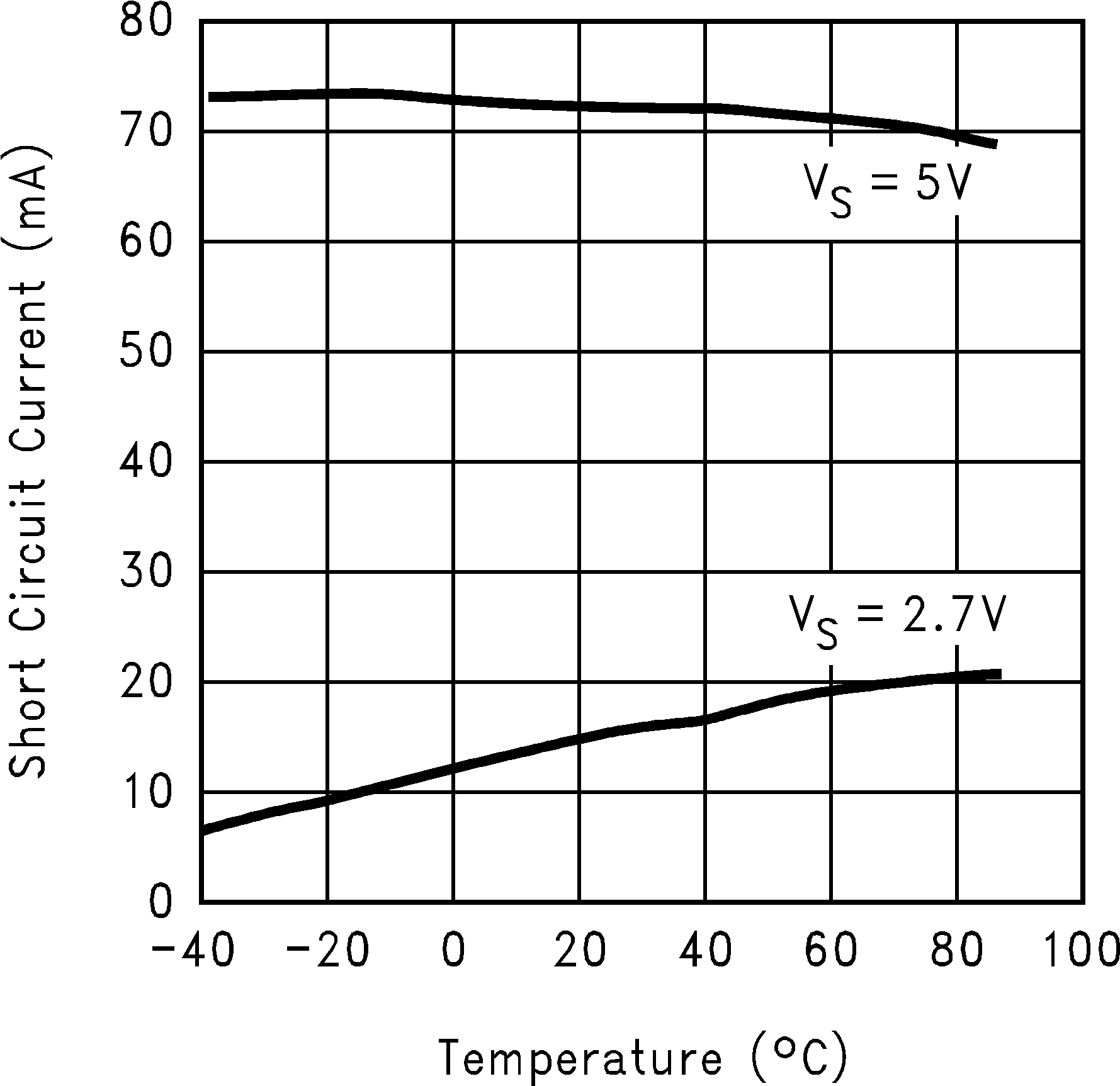 Figure 35. Short Circuit Current vs Temperature (Sinking)
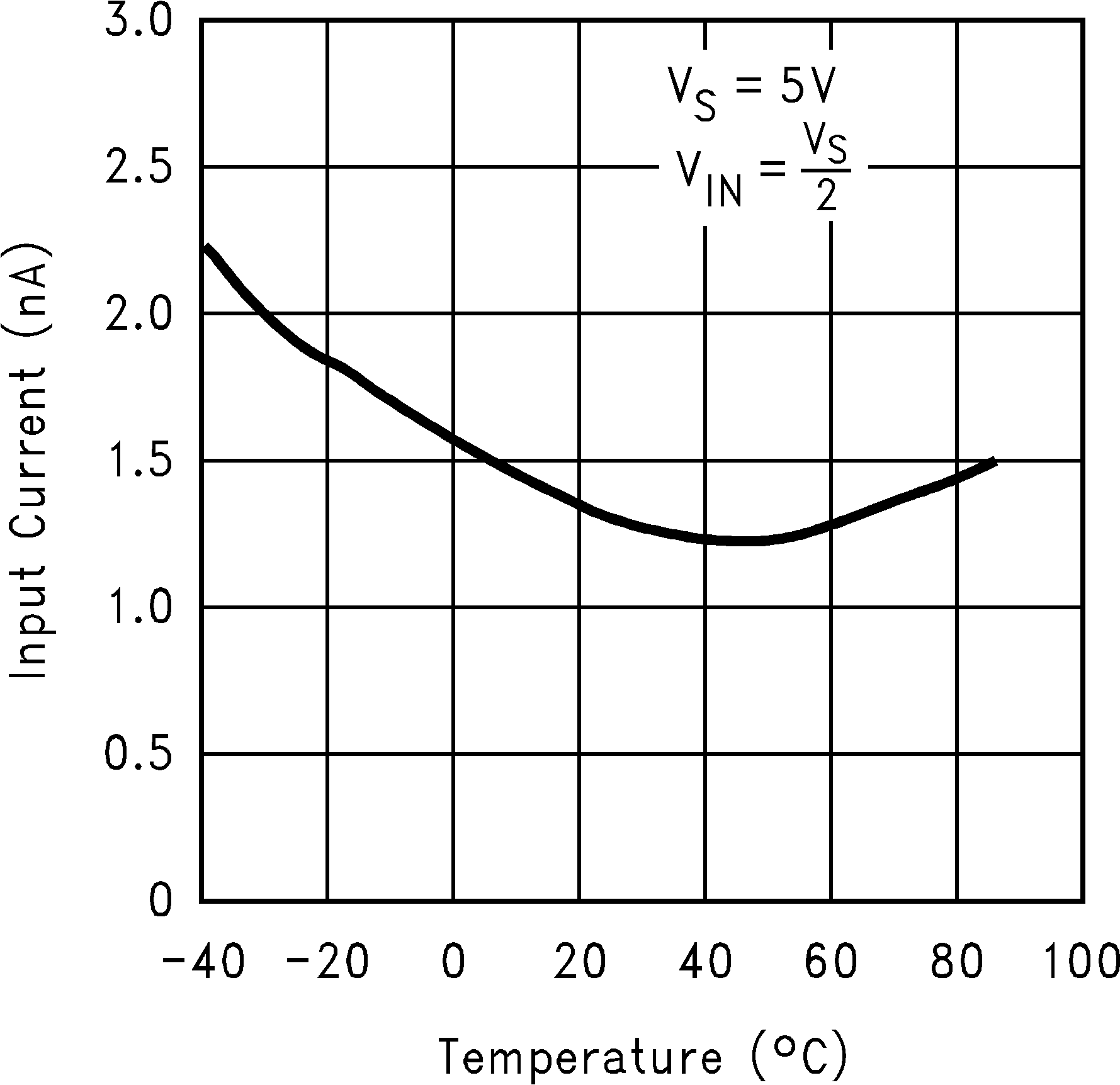 Figure 2. Input Current vs Temperature
 Figure 4. Sourcing Current vs Output Voltage
 Figure 6. Sinking Current vs Output Voltage
 Figure 8. Input Voltage Noise vs Frequency
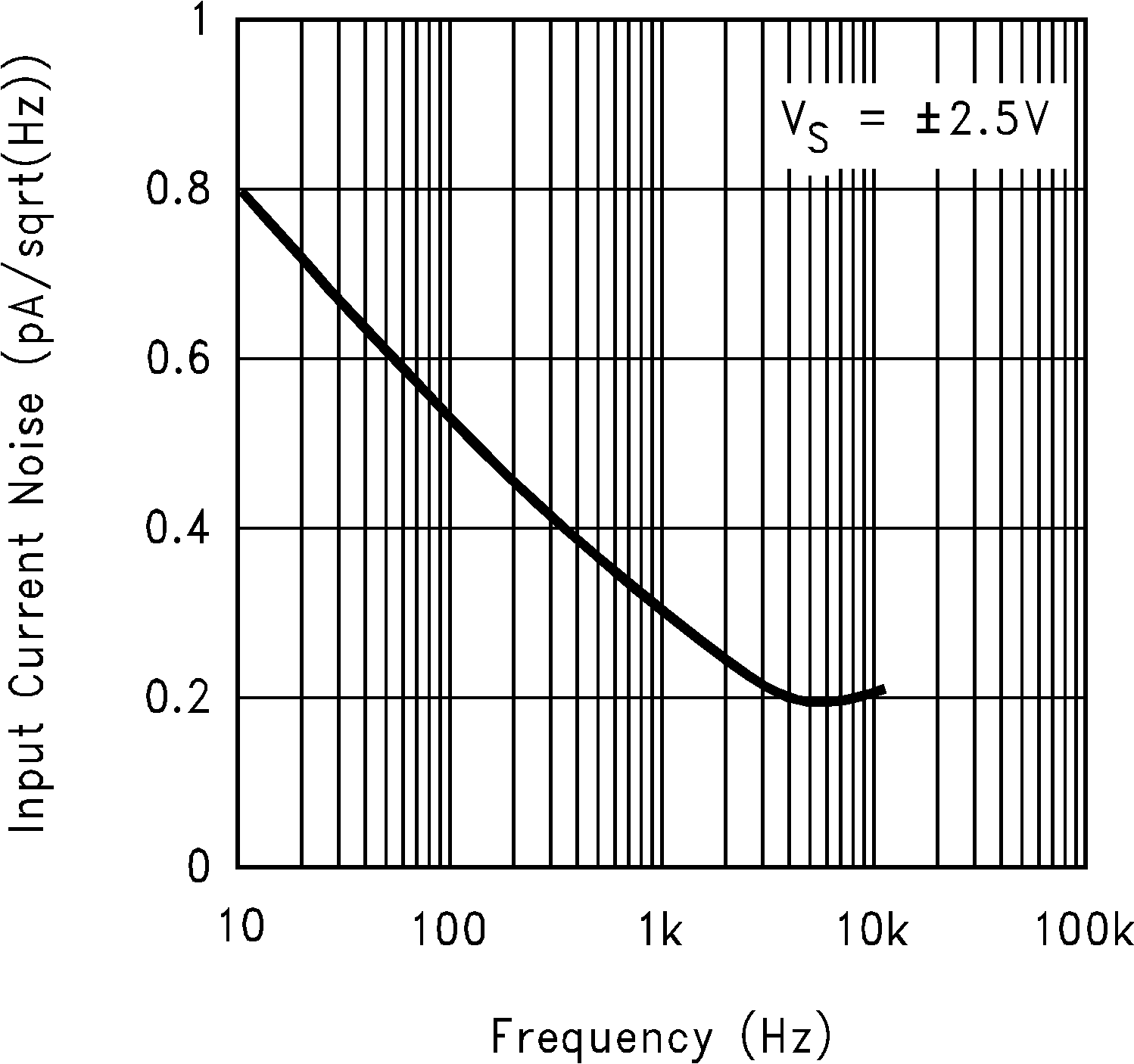 Figure 10. Input Current Noise vs Frequency
 Figure 12. PSRR vs Frequency
 Figure 14. CMRR vs Input Common Mode Voltage
 Figure 16. ΔVOS vs VCM
 Figure 18. Input Voltage vs Output Voltage
 Figure 20. Open-Loop Frequency Response
 Figure 22. Gain and Phase vs Capacitive Load
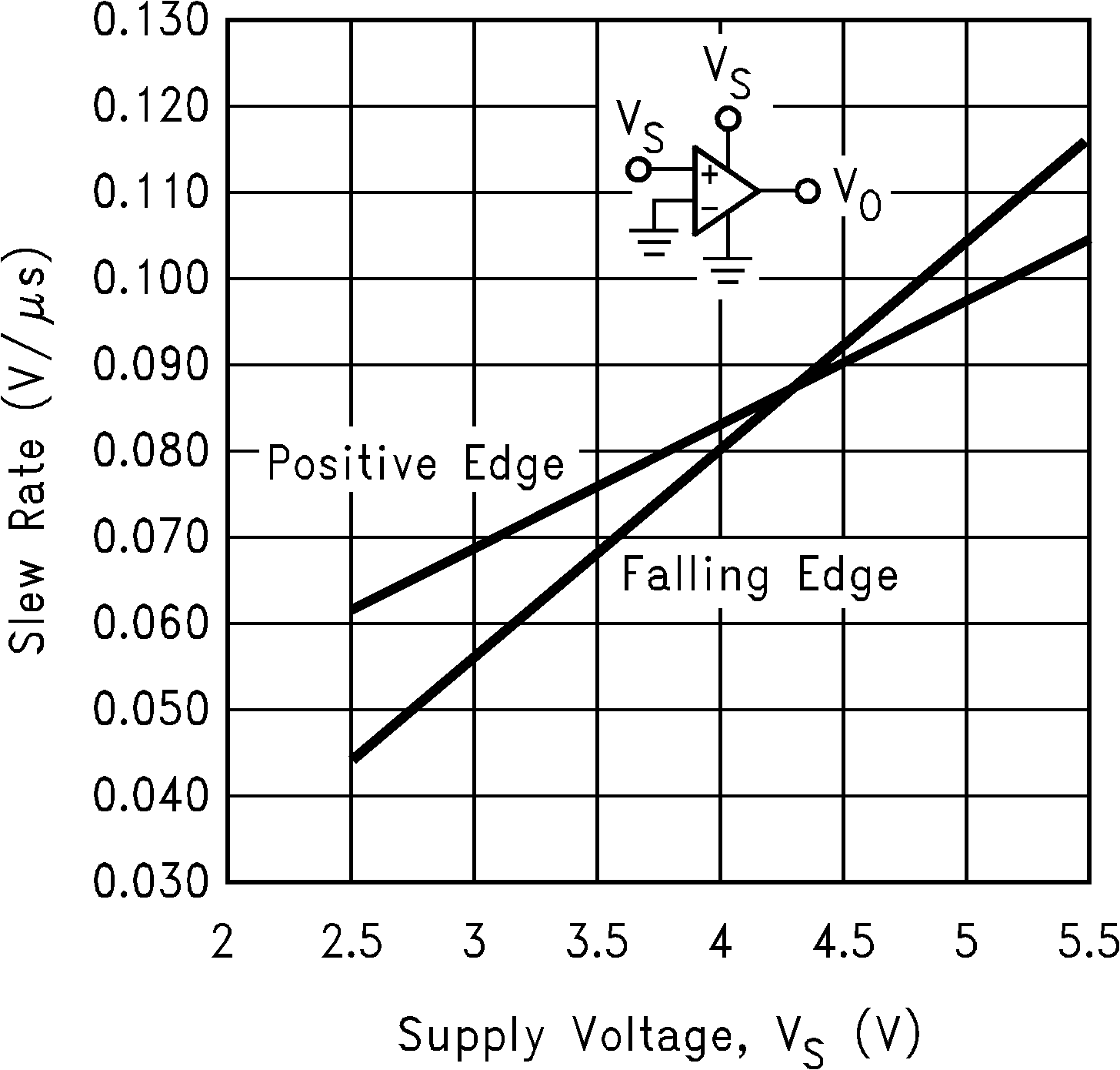 Figure 24. Slew Rate vs Supply Voltage
 Figure 26. Noninverting Small Signal Pulse Response
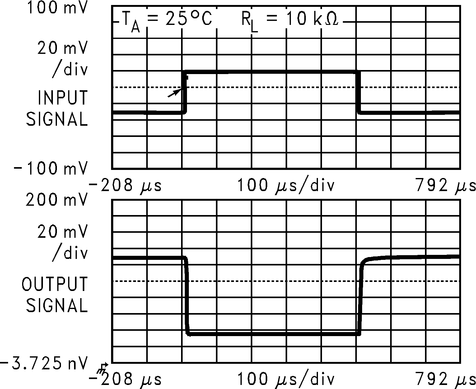 Figure 28. Inverting Small Signal Pulse Response
 Figure 30. Stability vs Capacitive Load
 Figure 32. Stability vs Capacitive Load
 Figure 34. Open-Loop Output Impedance vs Frequency
 Figure 36. Short Circuit Current vs Temperature (Sourcing)