JAJSA91D
August 2005 – August 2016
LPV511
PRODUCTION DATA.
1
特長
2
アプリケーション
3
概要
4
改訂履歴
5
Pin Configuration and Functions
6
Specifications
6.1
Absolute Maximum Ratings
6.2
ESD Ratings
6.3
Recommended Operating Conditions
6.4
Thermal Information
6.5
Electrical Characteristics: 3 V
6.6
Electrical Characteristics: 5 V
6.7
Electrical Characteristics: 12 V
6.8
Typical Characteristics
7
Detailed Description
7.1
Overview
7.2
Functional Block Diagram
7.3
Feature Description
7.4
Device Functional Modes
7.4.1
Input Stage
7.4.2
Output Stage
7.4.3
Driving Capacitive Load
8
Application and Implementation
8.1
Application Information
8.2
Typical Applications
8.2.1
Battery Current Sensing
8.2.1.1
Design Requirements
8.2.1.2
Detailed Design Procedure
8.2.1.3
Application Curve
8.2.2
Summing Amplifier
8.3
Dos and Don'ts
9
Power Supply Recommendations
10
Layout
10.1
Layout Guidelines
10.2
Layout Example
11
デバイスおよびドキュメントのサポート
11.1
デバイス・サポート
11.1.1
開発サポート
11.2
ドキュメントのサポート
11.2.1
関連資料
11.3
コミュニティ・リソース
11.4
商標
11.5
静電気放電に関する注意事項
11.6
Glossary
12
メカニカル、パッケージ、および注文情報
パッケージ・オプション
メカニカル・データ(パッケージ|ピン)
DCK|5
MPDS025J
サーマルパッド・メカニカル・データ
発注情報
jajsa91d_oa
jajsa91d_pm
10 Layout
10.1 Layout Guidelines
The V
+
pin should be bypassed to ground with a low-ESR capacitor.
The optimum placement is closest to the V
+
and ground pins.
Take care to minimize the loop area formed by the bypass capacitor connection between V
+
and ground.
The ground pin should be connected to the PCB ground plane at the pin of the device.
The feedback components should be placed as close to the device as possible minimizing strays.
10.2 Layout Example
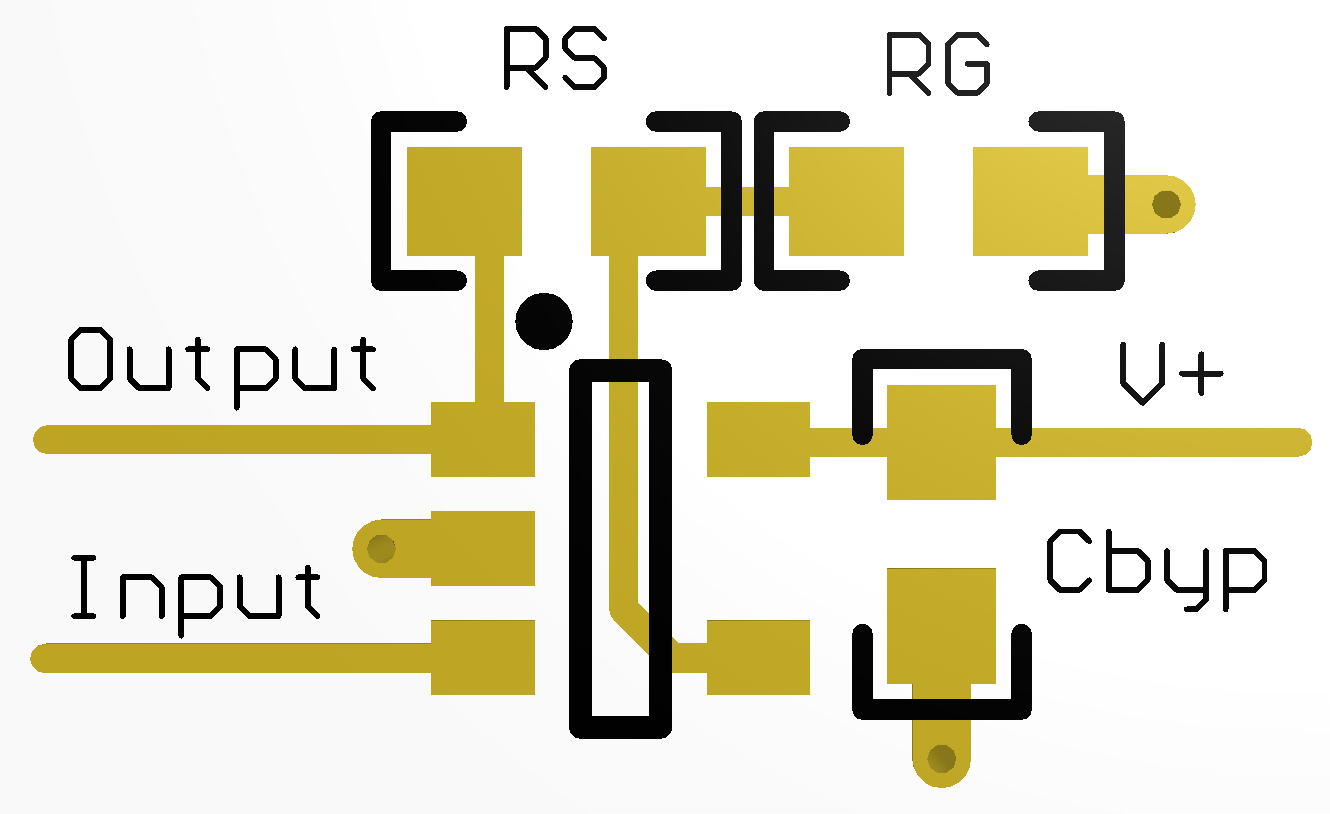
Figure 31. SOT-23 Layout Example