-
LPV542 Dual Nanopower 1.8 V, 490nA, RRIO CMOS Operational Amplifier
- 1 Features
- 2 Applications
- 3 Description
- 4 Revision History
- 5 Pin Configuration and Functions
- 6 Specifications
- 7 Detailed Description
- 8 Application and Implementation
- 9 Power Supply Recommendations
- 10Layout
- 11Device and Documentation Support
- 12Mechanical, Packaging, and Orderable Information
- IMPORTANT NOTICE
パッケージ・オプション
メカニカル・データ(パッケージ|ピン)
サーマルパッド・メカニカル・データ
発注情報
LPV542 Dual Nanopower 1.8 V, 490nA, RRIO CMOS Operational Amplifier
1 Features
- Wide Supply Range: 1.6 V to 5.5 V
- Low Supply Current: 490 nA (typical/channel)
- Good Offset Voltage: 3 mV (maximum/room)
- Good TcVos: 1µV/°C (typical)
- Gain-Bandwidth: 8 kHz (typical)
- Rail-to-Rail Input and Output
- Unity-Gain Stable
- Low Input Bias Current : 1 pA (typ)
- EMI Hardened
- Temperature Range: -40°C to 125°C
- Thin 3 mm x 3 mm x 0.45 mm X1SON package
2 Applications
- Wearables
- Personal Health Monitors
- Battery Packs
- Mobile Phones and Tablets
- Solar-Powered or Energy Harvested Systems
- PIR, Smoke, Gas, and Fire Detection Systems
- Battery Powered Internet of Things (IoT) Devices
- Remote Sensors
- Micropower Reference Buffer
3 Description
The LPV542 is an ultra-low-power, dual operational amplifier that provides 8kHz of bandwidth from 490nA of quiescent current making it well suited for battery-powered applications such as health and fitness wearables, building automation, and remote sensing nodes.
Each amplifier has a CMOS input stage with pico-amp bias currents which reduces errors commonly introduced in megaohm feedback resistance topologies such as photodiode and charge sense applications. In addition, the input common-mode range extends to the power supply rails and the output swings to within 3 mV of the rails, maintaining the widest dynamic range possible. Likewise, EMI protection is designed into the LPV542 in order to reduce system sensitivity to unwanted RF signals from mobile phones, WiFi, radio transmitters, and tag readers.
The LPV542 operates on a supply voltage as low as 1.6 V, ensuring continuous superior performance in low battery situations. The device is available in an 8-pad, low-profile, leadless 3 mm x 3 mm x 0.45 mm X1SON package and a standard 8 pin VSSOP.
Device Information(1)
| PART NUMBER | PACKAGE | BODY SIZE (NOM) |
|---|---|---|
| LPV542 | X1SON (8) | 3.00 mm x 3.00 mm |
| VSSOP (8) | 3.00 mm × 3.00 mm |
- For all available packages, see the orderable addendum at the end of the data sheet.
space
space
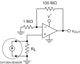
Nanopower Oxygen Sensor Amplifier

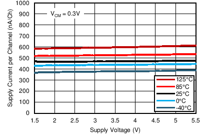
Supply Current vs. Supply Voltage

4 Revision History
Changes from * Revision (March 2015) to A Revision