SLVS033G February 1990 – July 2015 LT1054
PRODUCTION DATA.
- 1 Features
- 2 Applications
- 3 Description
- 4 Revision History
- 5 Pin Configuration and Functions
- 6 Specifications
- 7 Detailed Description
- 8 Application and Implementation
- 9 Power Supply Recommendations
- 10Layout
- 11Device and Documentation Support
- 12Mechanical, Packaging, and Orderable Information
パッケージ・オプション
デバイスごとのパッケージ図は、PDF版データシートをご参照ください。
メカニカル・データ(パッケージ|ピン)
- P|8
- DW|16
サーマルパッド・メカニカル・データ
- DW|16
発注情報
8 Application and Implementation
NOTE
Information in the following applications sections is not part of the TI component specification, and TI does not warrant its accuracy or completeness. TI’s customers are responsible for determining suitability of components for their purposes. Customers should validate and test their design implementation to confirm system functionality.
8.1 Application Information
The negative voltage converting and regulating ability of the LT1054 make this device optimal across a wide range of applications. As it is a regulator, there are many general design considerations that must be taken into account. Below will describe what to consider for using this device as a basic voltage inverter/regulator. This is the most common application for the LT1054 and the fundamental building block for the applications shown in System Examples.
8.2 Typical Application
8.2.1 Design Requirements
For this design example, use the parameters listed in Table 2 as the input parameters.
Table 2. Design Parameters
| Design Parameter | Example Value |
|---|---|
| Input Voltage Range | 3.5V to 15V |
| VOUT | -5V |
| IOUT | 100mA |
8.2.2 Detailed Design Procedure
When using LT1054 as a basic voltage inverter, determine the following:
- Input Voltage
- Desired output Voltage
- Desired Ripple
- Power Dissipation
8.2.2.1 Output Voltage Programming
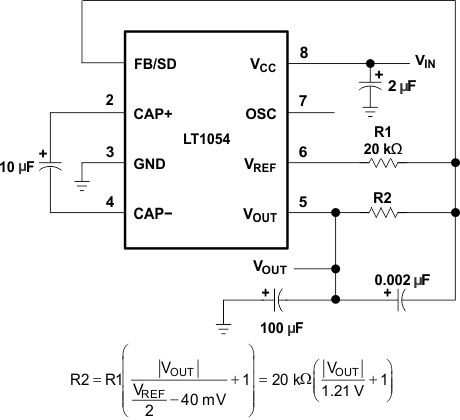
The error amplifier of the LT1054 drives the PNP switch to control the voltage across the input capacitor (CIN), which determines the output voltage. When the reference and error amplifier of the LT1054 are used, an external resistive divider is all that is needed to set the regulated output voltage. shows the basic regulator configuration and the formula for calculating the appropriate resistor values. R1 should be 20 kΩ or greater because the reference current is limited to ±100 μA. R2 should be in the range of 100 kΩ to 300 kΩ.
8.2.2.2 Capacitor Selection
While the exact values of CIN and COUT are noncritical, good-quality low-ESR capacitors, such as solid tantalum, are necessary to minimize voltage losses at high currents. For CIN, the effect of the ESR of the capacitor is multiplied by four, because switch currents are approximately two times higher than output current. Losses occur on both the charge and discharge cycle, which means that a capacitor with 1 Ω of ESR for CIN has the same effect as increasing the output impedance of the LT1054 by 4 Ω. This represents a significant increase in the voltage losses. COUT alternately is charged and discharged at a current approximately equal to the output current. The ESR of the capacitor causes a step function to occur in the output ripple at the switch transitions. This step function degrades the output regulation for changes in output load current and should be avoided. A technique used to gain both low ESR and reasonable cost is to parallel a smaller tantalum capacitor with a large aluminum electrolytic capacitor.
Frequency compensation is accomplished by adjusting the ratio of CIN to COUT.
For best results, this ratio should be approximately 1:10. Capacitor C1, required for good load regulation, should be 0.002 μF for all output voltages.
8.2.2.3 Output Ripple
The peak-to-peak output ripple is determined by the output capacitor and the output current values. Peak-to-peak output ripple is approximated as:

where
- ΔV = peak-to-peak ripple
- fOSC = oscillator frequency
For output capacitors with significant ESR, a second term must be added to account for the voltage step at the switch transitions. This step is approximately equal to:
8.2.2.4 Power Dissipation
The power dissipation of any LT1054 circuit must be limited so that the junction temperature of the device does not exceed the maximum junction-temperature ratings. The total power dissipation is calculated from two components–the power loss due to voltage drops in the switches, and the power loss due to drive-current losses. The total power dissipated by the LT1054 is calculated as:
where
- both VCC and VOUT are referenced to ground
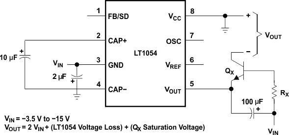
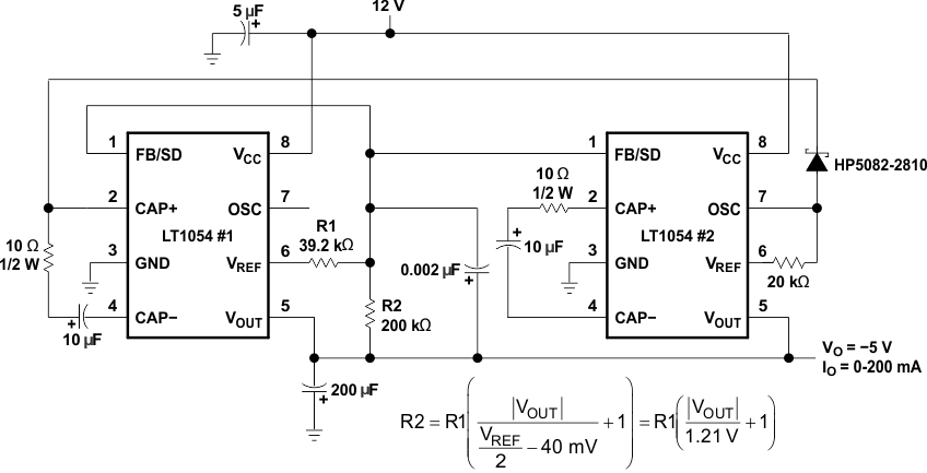
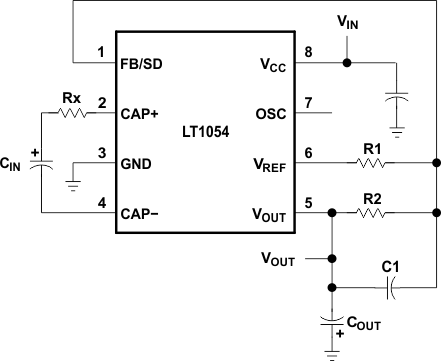
The power dissipation is equivalent to that of a linear regulator. Limited power-handling capability of the LT1054 packages causes limited output-current requirements, or steps can be taken to dissipate power external to the LT1054 for large input or output differentials. This is accomplished by placing a resistor in series with CIN as shown in Figure 16. A portion of the input voltage is dropped across this resistor without affecting the output regulation. Since switch current is approximately 2.2 times the output current and the resistor causes a voltage drop when CIN is both charging and discharging, the resistor chosen is as shown:

where
- VX ≈ VCC − [(LT1054 voltage loss)(1.3) + |VOUT|]
- IOUT = maximum required output current
The factor of 1.3 allows some operating margin for the LT1054.
When using a 12-V to −5-V converter at 100-mA output current, calculate the power dissipation without an external resistor.

At RθJA of 130°C/W for a commercial plastic device, a junction temperature rise of 122°C occurs. The device exceeds the maximum junction temperature at an ambient temperature of 25°C. To calculate the power dissipation with an external resistor (RX), determine how much voltage can be dropped across RX. The maximum voltage loss of the LT1054 in the standard regulator configuration at 100 mA output current is 1.6 V.
and

The resistor reduces the power dissipated by the LT1054 by (4.9 V)(100 mA) = 490 mW. The total power dissipated by the LT1054 is equal to (940 mW − 490 mW) = 450 mW. The junction-temperature rise is 58°C. Although commercial devices are functional up to a junction temperature of 125°C, the specifications are tested to a junction temperature of 100°C. In this example, this means limiting the ambient temperature to 42°C. To allow higher ambient temperatures, the thermal resistance numbers for the LT1054 packages represent worst-case numbers, with no heat sinking and still air. Small clip-on heat sinks can be used to lower the thermal resistance of the LT1054 package. Airflow in some systems helps to lower the thermal resistance. Wide printed circuit board traces from the LT1054 leads help remove heat from the device. This is especially true for plastic packages.
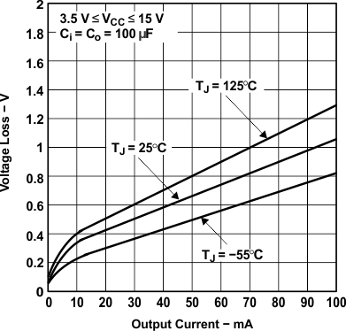
8.2.3 Application Curve
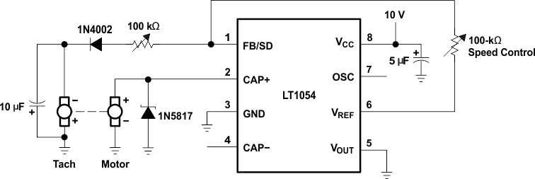
8.3 System Examples
NOTE:
Motor-Tach is Canon CKT26-T5-3SAE.