SLVS033G February 1990 – July 2015 LT1054
PRODUCTION DATA.
- 1 Features
- 2 Applications
- 3 Description
- 4 Revision History
- 5 Pin Configuration and Functions
- 6 Specifications
- 7 Detailed Description
- 8 Application and Implementation
- 9 Power Supply Recommendations
- 10Layout
- 11Device and Documentation Support
- 12Mechanical, Packaging, and Orderable Information
パッケージ・オプション
デバイスごとのパッケージ図は、PDF版データシートをご参照ください。
メカニカル・データ(パッケージ|ピン)
- P|8
- DW|16
サーマルパッド・メカニカル・データ
- DW|16
発注情報
10 Layout
10.1 Layout Guidelines
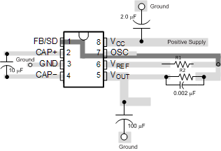
- Try to run the feedback trace as far from the noisy power or clocking traces as possible. In the case that the OSC pin is not being used, as in Figure 31, the FB trace can be ran on a lower layer under the OSC pin. When OSC is being utilized by a noisy clocking signal, it is recommended to run the FB trace on a lower layer through the Vref pin.
- Keep the FB trace to be as direct as possible and somewhat thick. These two sometimes involve a trade-off, but keeping it away from EMI and other noise sources is the more critical of the two.
- Keep the external capacitor traces short, specifically on the CAP+ and CAP- nodes that have the fastest rise and fall times.
- Make all of the power (high current) traces as short, direct, and thick as possible. It is good practice on a standard PCB board to make the traces an absolute minimum of 15 mils (0.381 mm) per Ampere.
10.2 Layout Example
 Figure 31. Basic Inverter/Regulator Layout