SLVS033G February 1990 – July 2015 LT1054
PRODUCTION DATA.
- 1 Features
- 2 Applications
- 3 Description
- 4 Revision History
- 5 Pin Configuration and Functions
- 6 Specifications
- 7 Detailed Description
- 8 Application and Implementation
- 9 Power Supply Recommendations
- 10Layout
- 11Device and Documentation Support
- 12Mechanical, Packaging, and Orderable Information
パッケージ・オプション
デバイスごとのパッケージ図は、PDF版データシートをご参照ください。
メカニカル・データ(パッケージ|ピン)
- P|8
- DW|16
サーマルパッド・メカニカル・データ
- DW|16
発注情報
9 Power Supply Recommendations
The LT1054 alternately charges CIN to the input voltage when CIN is switched in parallel with the input supply and then transfers charge to COUT when CIN is switched in parallel with COUT. Switching occurs at the oscillator frequency. During the time that CIN is charging, the peak supply current will be approximately equal to 2.2 times the output current. During the time that CIN is delivering charge to COUT the supply current drops to approximately 0.2 times the output current. An input supply bypass capacitor will supply part of the peak input current drawn by the LT1054 and average out the current drawn from the supply. A minimum input supply bypass capacitor of 2µF, preferably tantalum or some other low ESR type is recommended. A larger capacitor may be desirable in some cases, for example, when the actual input supply is connected to the LT1054 through long leads, or when the pulse current drawn by the LT1054 might affect other circuitry through supply coupling.
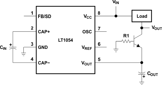
In addition to being the output terminal, VOUT is tied to the substrate of the device. Special care must be taken in LT1054 circuits to avoid making VOUT positive with respect to any of the other terminals. For circuits with the output load connected from VCC to VOUT or from some external positive supply voltage to VOUT, an external transistor must be added (see Figure 30). This transistor prevents VOUT from being pulled above GND during startup. Any small general-purpose transistor such as a 2N2222 or a 2N2219 device can be used. Resistor R1 should be chosen to provide enough base drive to the external transistor so that it is saturated under nominal output voltage and maximum output current conditions.

 Figure 30. Circuit With Load Connected from VCC to VOUT