JAJSST5A June 2015 – February 2024 LV14540
PRODUCTION DATA
- 1
- 1 特長
- 2 アプリケーション
- 3 概要
- 4 Pin Configuration and Functions
- 5 Specifications
-
6 Detailed Description
- 6.1 Overview
- 6.2 Functional Block Diagram
- 6.3
Feature Description
- 6.3.1 Fixed Frequency Peak Current Mode Control
- 6.3.2 Slope Compensation
- 6.3.3 Pulse Skipping Mode
- 6.3.4 Low Dropout Operation and Bootstrap Voltage (BOOT)
- 6.3.5 Adjustable Output Voltage
- 6.3.6 Enable and Adjustable Undervoltage Lockout
- 6.3.7 External Soft Start
- 6.3.8 Switching Frequency and Synchronization (RT/SYNC)
- 6.3.9 Overcurrent and Short-Circuit Protection
- 6.3.10 Overvoltage Protection
- 6.3.11 Thermal Shutdown
- 6.4 Device Functional Modes
- 7 Application and Implementation
- 8 Device and Documentation Support
- 9 Revision History
- 10Mechanical, Packaging, and Orderable Information
6.3.8 Switching Frequency and Synchronization (RT/SYNC)
The switching frequency of the LV14540 can be programmed by the resistor RT from the RT/SYNC pin and GND pin. The RT/SYNC pin cannot be left floating or shorted to ground. To determine the timing resistance for a given switching frequency, use Equation 5 or the curve in Figure 6-4. Table 6-1 gives typical RT values for a given fSW.
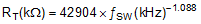
 Figure 6-4 RT versus Frequency Curve
| fSW (kHz) | RT (kΩ) |
|---|---|
| 200 | 133 |
| 350 | 73.2 |
| 500 | 49.9 |
| 750 | 32.4 |
| 1000 | 23.2 |
| 1500 | 15.0 |
| 1912 | 11.5 |
| 2000 | 11.0 |
The LV14540 switching action can also be synchronized to an external clock from 250 kHz to 2 MHz. Connect a square wave to the RT/SYNC pin through either circuit network shown in Figure 6-5. The internal oscillator is synchronized by the falling edge of the external clock. The recommendations for the external clock include a high level no lower than 1.7 V, a low level no higher than 0.5 V, and a pulse width greater than 30 ns. When using a low impedance signal source, the frequency setting resistor RT is connected in parallel with an AC coupling capacitor CCOUP to termination resistor RTERM (for example, 50 Ω). The two resistors in series provide the default frequency setting resistance when the signal source is turned off. A 470 pF ceramic capacitor can be used for CCOUP. Figure 6-6, Figure 6-7, and Figure 6-8 show the device synchronized to an external system clock.
 Figure 6-5 Synchronizing to an External Clock
 Figure 6-6 Synchronizing in CCM
 Figure 6-8 Synchronizing in PSM
 Figure 6-7 Synchronizing in DCM
Equation 6 calculates the maximum switching frequency limitation set by the minimum controllable on time and the input to output step-down ratio. Setting the switching frequency above this value causes the regulator to skip switching pulses to achieve the low duty cycle required at maximum input voltage.
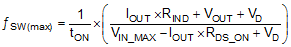
where
- IOUT = Output current
- RIND = Inductor series resistance
- VIN_MAX = Maximum input voltage
- VOUT = Output voltage
- VD = Diode voltage drop
- RDS_ON = High-side MOSFET switch on resistance
- tON = Minimum on-time