JAJSST5A June 2015 – February 2024 LV14540
PRODUCTION DATA
- 1
- 1 特長
- 2 アプリケーション
- 3 概要
- 4 Pin Configuration and Functions
- 5 Specifications
-
6 Detailed Description
- 6.1 Overview
- 6.2 Functional Block Diagram
- 6.3
Feature Description
- 6.3.1 Fixed Frequency Peak Current Mode Control
- 6.3.2 Slope Compensation
- 6.3.3 Pulse Skipping Mode
- 6.3.4 Low Dropout Operation and Bootstrap Voltage (BOOT)
- 6.3.5 Adjustable Output Voltage
- 6.3.6 Enable and Adjustable Undervoltage Lockout
- 6.3.7 External Soft Start
- 6.3.8 Switching Frequency and Synchronization (RT/SYNC)
- 6.3.9 Overcurrent and Short-Circuit Protection
- 6.3.10 Overvoltage Protection
- 6.3.11 Thermal Shutdown
- 6.4 Device Functional Modes
- 7 Application and Implementation
- 8 Device and Documentation Support
- 9 Revision History
- 10Mechanical, Packaging, and Orderable Information
6.3.6 Enable and Adjustable Undervoltage Lockout
The LV14540 is enabled when the VIN pin voltage rises above 3.7 V (typical) and the EN pin voltage exceeds the enable threshold of 1.2 V (typical). The LV14540 is disabled when the VIN pin voltage falls below 3.42 V (typical) or when the EN pin voltage is below 1.2 V. The EN pin has an internal pullup current source (typically IEN = 1 μA) that enables operation of the LV14540 when the EN pin is floating.
Many applications will benefit from the employment of an enable divider RENT and RENB in Figure 6-3 to establish a precision system UVLO level for the stage. System UVLO can be used for supplies operating from utility power as well as battery power. It can be used for sequencing, making sure of reliable operation, or supply protection, such as a battery. An external logic signal can also be used to drive EN input for system sequencing and protection.
When EN terminal voltage exceeds 1.2 V, an additional hysteresis current (typically IHYS = 3.6 μA) is sourced out of the EN terminal. When the EN terminal is pulled below 1.2 V, IHYS current is removed. This additional current facilitates adjustable input voltage UVLO hysteresis. Use Equation 2 and Equation 3 to calculate RENT and RENB for desired UVLO hysteresis voltage.
 Figure 6-3 System UVLO by Enable Dividers
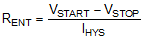
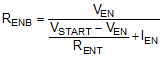
where VSTART is the desired voltage threshold to enable LV14540, VSTOP is the desired voltage threshold to disable device.