JAJSMD7D October 2005 – July 2024 MAX3221E
PRODUCTION DATA
- 1
- 1 特長
- 2 アプリケーション
- 3 概要
- 4 Pin Configuration and Functions
-
5 Specifications
- 5.1 Absolute Maximum Ratings
- 5.2 ESD Ratings
- 5.3 ESD Ratings - IEC Specifications
- 5.4 Recommended Operating Conditions
- 5.5 Thermal Information
- 5.6 Electrical Characteristics
- 5.7 Electrical Characteristics: Driver
- 5.8 Electrical Characteristics: Receiver
- 5.9 Electrical Characteristics: Auto-Power Down
- 5.10 Switching Characteristics: Driver
- 5.11 Switching Characteristics: Receiver
- 5.12 Switching Characteristics: Auto-Power Down
- 5.13 代表的特性
- 6 Parameter Measurement Information
- 7 Detailed Description
- 8 Application and Implementation
- 9 Device and Documentation Support
- 10Revision History
- 11Mechanical, Packaging, and Orderable Information
パッケージ・オプション
メカニカル・データ(パッケージ|ピン)
サーマルパッド・メカニカル・データ
発注情報
4 Pin Configuration and Functions
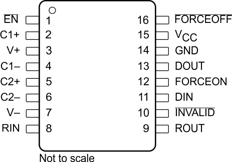
 Figure 4-1 DB or PW Package
16-Pin SSOP or TSSOP
(Top View)
Table 4-1 Pin Functions
| PIN | I/O | DESCRIPTION | |
|---|---|---|---|
| NAME | NO. | ||
| C1+ | 2 | — | Positive terminals of the voltage-doubler charge pump capacitors |
| C2+ | 5 | ||
| C1– | 4 | — | Negative terminals of the voltage-doubler charge pump capacitors |
| C2– | 6 | ||
| DIN | 11 | I | Driver input |
| DOUT | 13 | O | RS-232 driver output |
| EN | 1 | I | Low input enables receiver ROUT output. High input sets ROUT to high impedance. |
| FORCEOFF | 16 | I | Automatic power-down control input |
| FORCEON | 12 | I | Automatic power-down control input |
| GND | 14 | — | Ground |
| INVALID | 10 | O | Invalid output pin. Output low when RIN input is unpowered. |
| RIN | 8 | I | RS-232 receiver input |
| ROUT | 9 | O | Receiver output |
| VCC | 15 | — | 3V to 5.5V supply voltage |
| V+ | 3 | O | 5.5V supply generated by the charge pump |
| V– | 7 | O | –5.5V supply generated by the charge pump |