SLLS408H January 2000 – October 2016 MAX3222
PRODUCTION DATA.
- 1 Features
- 2 Applications
- 3 Description
- 4 Revision History
- 5 Pin Configuration and Functions
-
6 Specifications
- 6.1 Absolute Maximum Ratings
- 6.2 ESD Ratings
- 6.3 Recommended Operating Conditions
- 6.4 Thermal Information
- 6.5 Electrical Characteristics: Device
- 6.6 Electrical Characteristics: Driver
- 6.7 Electrical Characteristics: Receiver
- 6.8 Switching Characteristics: Driver
- 6.9 Switching Characteristics: Receiver
- 6.10 Typical Characteristics
- 7 Parameter Measurement Information
- 8 Detailed Description
- 9 Application and Implementation
- 10Power Supply Recommendations
- 11Layout
- 12Device and Documentation Support
- 13Mechanical, Packaging, and Orderable Information
パッケージ・オプション
デバイスごとのパッケージ図は、PDF版データシートをご参照ください。
メカニカル・データ(パッケージ|ピン)
- DB|20
- PW|20
- DW|20
サーマルパッド・メカニカル・データ
発注情報
8 Detailed Description
8.1 Overview
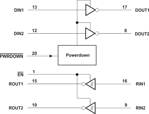
The MAX3222 consists of two line drivers, two line receivers, and a dual charge-pump circuit with ±15-kV ESD protection pin to pin (serial-port connection pins, including GND). The device meets the requirements of TIA/EIA-232-F and provides the electrical interface between an asynchronous communication controller and the serial-port connector. The charge pump and four small external capacitors allow operation from a single 3-V to 5.5-V supply. The device operates at data signaling rates up to 250 kbit/s and a maximum of 30-V/μs driver output slew rate.
The MAX3222 can be placed in the power-down mode by setting PWRDOWN low, which draws only 1 μA from the power supply. When the device is powered down, the receivers remain active while the drivers are placed in the high-impedance state. Also, during power down, the onboard charge pump is disabled; V+ is lowered to VCC, and V− is raised toward GND. Receiver outputs also can be placed in the high-impedance state by setting EN high.
8.2 Functional Block Diagram
 Figure 7. Logic Diagram (Positive Logic)
8.3 Feature Description
8.3.1 Power
The power block increases, inverts, and regulates voltage at V+ and V- pins using a charge pump that requires four external capacitors.
8.3.2 RS232 Driver
Two drivers interface standard logic level to RS232 levels. PWRDOWN input low turns driver off and PWRDOWN input high turns driver on. Both DIN inputs and PWRDOWN input must be valid high or low. Do not float logic input pins.
8.3.3 RS232 Receiver
Two receivers interface RS232 levels to standard logic levels. An open input will result in a high output on ROUT. Each RIN input includes an internal standard RS232 load. EN input low turns on both ROUT pins. EN input high puts both ROUT pins into high impedance state, output off. EN input must be valid high or low. Do not float logic input pins.
8.4 Device Functional Modes
Driver and receiver outputs are controlled by the functional truth tables.
Table 1. Functional Table - Each Driver(1)
| INPUTS | OUTPUT DOUT | |
|---|---|---|
| DIN | PWRDOWN | |
| X | L | Z |
| L | H | H |
| H | H | L |
Table 2. Functional Table - Each Receiver(1)
| INPUTS | OUTPUT ROUT | |
|---|---|---|
| RIN | EN | |
| L | L | H |
| H | L | L |
| X | H | Z |
| Open | L | H |