SLLS408H January 2000 – October 2016 MAX3222
PRODUCTION DATA.
- 1 Features
- 2 Applications
- 3 Description
- 4 Revision History
- 5 Pin Configuration and Functions
-
6 Specifications
- 6.1 Absolute Maximum Ratings
- 6.2 ESD Ratings
- 6.3 Recommended Operating Conditions
- 6.4 Thermal Information
- 6.5 Electrical Characteristics: Device
- 6.6 Electrical Characteristics: Driver
- 6.7 Electrical Characteristics: Receiver
- 6.8 Switching Characteristics: Driver
- 6.9 Switching Characteristics: Receiver
- 6.10 Typical Characteristics
- 7 Parameter Measurement Information
- 8 Detailed Description
- 9 Application and Implementation
- 10Power Supply Recommendations
- 11Layout
- 12Device and Documentation Support
- 13Mechanical, Packaging, and Orderable Information
パッケージ・オプション
デバイスごとのパッケージ図は、PDF版データシートをご参照ください。
メカニカル・データ(パッケージ|ピン)
- DB|20
- PW|20
- DW|20
サーマルパッド・メカニカル・データ
発注情報
11 Layout
11.1 Layout Guidelines
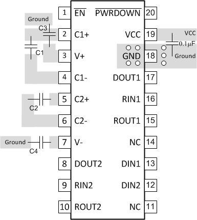
Keep the external capacitor traces short. This is more important on C1 and C2 nodes that have the fastest rise and fall times. Make the impedance from MAX3222 ground pin and circuit board's ground plane as low as possible for best ESD performance. Use wide metal and multiple vias on both sides of ground pin
11.2 Layout Example
 Figure 11. MAX3222 Layout