SLLS408H January 2000 – October 2016 MAX3222
PRODUCTION DATA.
- 1 Features
- 2 Applications
- 3 Description
- 4 Revision History
- 5 Pin Configuration and Functions
-
6 Specifications
- 6.1 Absolute Maximum Ratings
- 6.2 ESD Ratings
- 6.3 Recommended Operating Conditions
- 6.4 Thermal Information
- 6.5 Electrical Characteristics: Device
- 6.6 Electrical Characteristics: Driver
- 6.7 Electrical Characteristics: Receiver
- 6.8 Switching Characteristics: Driver
- 6.9 Switching Characteristics: Receiver
- 6.10 Typical Characteristics
- 7 Parameter Measurement Information
- 8 Detailed Description
- 9 Application and Implementation
- 10Power Supply Recommendations
- 11Layout
- 12Device and Documentation Support
- 13Mechanical, Packaging, and Orderable Information
パッケージ・オプション
デバイスごとのパッケージ図は、PDF版データシートをご参照ください。
メカニカル・データ(パッケージ|ピン)
- DB|20
- PW|20
- DW|20
サーマルパッド・メカニカル・データ
発注情報
6 Specifications
6.1 Absolute Maximum Ratings
over operating free-air temperature range (unless otherwise noted)(1)| MIN | MAX | UNIT | ||
|---|---|---|---|---|
| Supply voltage, VCC(2) | –0.3 | 6 | V | |
| Positive output supply voltage, V+(2) | –0.3 | 7 | V | |
| Negative output supply voltage, V–(2) | 0.3 | -7 | V | |
| Supply voltage difference, V+ – V– | 13 | V | ||
| Input voltage, VI | Drivers, EN, PWRDOWN | –0.3 | 6 | V |
| Receiver | –25 | 25 | ||
| Output voltage, VO | Drivers | –13.2 | 13.2 | V |
| Receivers | –0.3 | VCC + 0.3 | ||
| Operating virtual junction temperature, TJ | 150 | °C | ||
| Storage temperature, Tstg | –65 | 150 | °C | |
(1) Stresses beyond those listed under Absolute Maximum Ratings may cause permanent damage to the device. These are stress ratings only, which do not imply functional operation of the device at these or any other conditions beyond those indicated under Recommended Operating Conditions. Exposure to absolute-maximum-rated conditions for extended periods may affect device reliability.
(2) All voltages are with respect to network GND.
6.2 ESD Ratings
| VALUE | UNIT | ||||
|---|---|---|---|---|---|
| V(ESD) | Electrostatic discharge | Human-body model (HBM), per ANSI/ESDA/JEDEC JS-001 RIN, DOUT, and GND pins (1) |
Pins 8, 9, 16, 17 and 18 | ±15000 | V |
| All other pins | ±3000 | ||||
| Charged-device model (CDM), per JEDEC specification JESD22-C101(2) | All pins | ±1500 | |||
(1) JEDEC document JEP155 states that 500-V HBM allows safe manufacturing with a standard ESD control process.
(2) JEDEC document JEP157 states that 250-V CDM allows safe manufacturing with a standard ESD control process.
6.3 Recommended Operating Conditions
over operating free-air temperature range (unless otherwise noted)(1). See Figure 8.| MIN | NOM | MAX | UNIT | ||||
|---|---|---|---|---|---|---|---|
| Supply voltage | VCC = 3.3 V | 3 | 3.3 | 3.6 | V | ||
| VCC = 5 V | 4.5 | 5 | 5.5 | ||||
| VIH | Driver and control high-level input voltage | DIR, EN, PWRDOWN | VCC = 3.3 V | 2 | V | ||
| VCC = 5 V | 2.4 | ||||||
| VIL | Driver and control low-level input voltage | DIR, EN, PWRDOWN | 0.8 | V | |||
| VI | Driver and control input voltage | DIR, EN, PWRDOWN | 0 | 5.5 | V | ||
| VI | Receiver input voltage | –25 | 25 | V | |||
| TA | Operating free-air temperature | MAX3222C | 0 | 70 | ºC | ||
| MAX3222I | –40 | 85 | |||||
(1) Test conditions are C1−C4 = 0.1 μF at VCC = 3.3 V ± 0.3 V; C1 = 0.047 μF, C2−C4 = 0.33 μF at VCC = 5 V ± 0.5 V.
6.4 Thermal Information
| THERMAL METRIC(1)(2)(3) | MAX3222 | UNIT | |||
|---|---|---|---|---|---|
| DB (SSOP) | DW (SOIC) | PW (TSSOP) | |||
| 20 PINS | 20 PINS | 20 PINS | |||
| RθJA | Junction-to-ambient thermal resistance | 84.4 | 70.2 | 94.3 | °C/W |
| RθJC(top) | Junction-to-case (top) thermal resistance | 44.1 | 36.2 | 29.9 | °C/W |
| RθJB | Junction-to-board thermal resistance | 40 | 37.9 | 45.1 | °C/W |
| ψJT | Junction-to-top characterization parameter | 11 | 11.1 | 1.4 | °C/W |
| ψJB | Junction-to-board characterization parameter | 39.5 | 37.5 | 44.6 | °C/W |
(1) For more information about traditional and new thermal metrics, see the Semiconductor and IC Package Thermal Metrics application report.
(2) Maximum power dissipation is a function of TJ(max), θJA, and TA. The maximum allowable power dissipation at any allowable ambient temperature is PD = (TJ(max) − TA)/θJA. Operating at the absolute maximum TJ of 150°C can affect reliability.
(3) The package thermal impedance is calculated in accordance with JESD 51-7.
6.5 Electrical Characteristics: Device
over operating free-air temperature range (unless otherwise noted)(2). See Figure 8.| PARAMETER | TEST CONDITIONS | MIN | TYP(1) | MAX | UNIT | |
|---|---|---|---|---|---|---|
| II | Input leakage current (EN, PWRDOWN) | ±0.01 | ±1 | µA | ||
| ICC | Supply current | No load, PWRDOWN at VCC | 0.3 | 1 | mA | |
| Supply current (powered off) | No load, PWRDOWN at GND | 1 | 10 | µA | ||
(1) All typical values are at VCC = 3.3 V or VCC = 5 V, and TA = 25°C.
(2) Test conditions are C1−C4 = 0.1 μF at VCC = 3.3 V ± 0.3 V; C1 = 0.047 μF, C2−C4 = 0.33 μF at VCC = 5 V ± 0.5 V.
6.6 Electrical Characteristics: Driver
over operating free-air temperature range (unless otherwise noted)(2). See Figure 8.| PARAMETER | TEST CONDITIONS | MIN | TYP(1) | MAX | UNIT | |
|---|---|---|---|---|---|---|
| VOH | High-level output voltage | DOUT at RL = 3 kΩ to GND, DIN = GND | 5 | 5.4 | V | |
| VOL | Low-level output voltage | DOUT at RL = 3 kΩ to GND, DIN = VCC | –5 | –5.4 | V | |
| IIH | High-level input current | VI = VCC | ±0.01 | ±1 | µA | |
| IIL | Low-level input current | VI at GND | ±0.01 | ±1 | µA | |
| IOS | Short-circuit output current | VCC = 3.6 V, VO = 0 V | ±35 | ±60 | mA | |
| VCC = 5.5 V, VO = 0 V | ||||||
| ro | Output resistance | VCC, V+, and V– = 0 V, VO = ±2 V | 300 | 10M | Ω | |
| Ioff | Output leakage current | PWRDOWN = GND, VO = ±12 V, VCC = 3 V to 3.6 V | ±25 | µA | ||
| PWRDOWN = GND, VO = ±10 V, VCC = 4.5 V to 5.5 V | ±25 | |||||
(1) All typical values are at VCC = 3.3 V or VCC = 5 V, and TA = 25°C.
(2) Test conditions are C1−C4 = 0.1 μF at VCC = 3.3 V ± 0.3 V; C1 = 0.047 μF, C2−C4 = 0.33 μF at VCC = 5 V ± 0.5 V.
6.7 Electrical Characteristics: Receiver
over operating free-air temperature range (unless otherwise noted)(2). See Figure 8.| PARAMETER | TEST CONDITIONS | MIN | TYP(1) | MAX | UNIT | |
|---|---|---|---|---|---|---|
| VOH | High-level output voltage | IOH = –1 mA | VCC – 0.6 | VCC – 0.1 | V | |
| VOL | Low-level output voltage | IOL = 1.6 mA | 0.4 | V | ||
| VIT+ | Positive-going input threshold voltage | VCC = 3.3 V | 1.5 | 2.4 | V | |
| VCC = 5 V | 1.8 | 2.4 | ||||
| VIT– | Negative-going input threshold voltage | VCC = 3.3 V | 0.6 | 1.2 | V | |
| VCC = 5 V | 0.8 | 1.5 | ||||
| Vhys | Input hysteresis (VIT+ – VIT–) | 0.3 | V | |||
| Ioff | Output leakage current | EN = VCC | ±0.05 | ±10 | µA | |
| ri | Input resistance | VI = ±3 V to ±25 V | 3 | 5 | 7 | kΩ |
(1) All typical values are at VCC = 3.3 V or VCC = 5 V, and TA = 25°C.
(2) Test conditions are C1−C4 = 0.1 μF at VCC = 3.3 V ± 0.3 V; C1 = 0.047 μF, C2−C4 = 0.33 μF at VCC = 5 V ± 0.5 V.
6.8 Switching Characteristics: Driver
over operating free-air temperature range (unless otherwise noted)(3). See Figure 8.| PARAMETER | TEST CONDITIONS | MIN | TYP(1) | MAX | UNIT | ||
|---|---|---|---|---|---|---|---|
| Maximum data rate | CL = 1000 pF, RL = 3 kΩ, One DOUT switching, see Figure 3 | 150 | 250 | kbps | |||
| tsk(p) | Pulse skew(2) | CL = 150 pF to 2500 pF, RL = 3 kΩ to 7 kΩ, see Figure 4 | 300 | ns | |||
| SR(tr) | Slew rate, transition region (see Figure 3) | RL = 3 kΩ to 7 kΩ, VCC = 3.3 V | CL = 150 pF to 1000 pF | 6 | 30 | V/µs | |
| CL = 150 pF to 2500 pF | 4 | 30 | |||||
(1) All typical values are at VCC = 3.3 V or VCC = 5 V, and TA = 25°C.
(2) Pulse skew is defined as |tPLH − tPHL| of each channel of the same device.
(3) Test conditions are C1−C4 = 0.1 μF at VCC = 3.3 V ± 0.3 V; C1 = 0.047 μF, C2−C4 = 0.33 μF at VCC = 5 V ± 0.5 V.
6.9 Switching Characteristics: Receiver
over operating free-air temperature range (unless otherwise noted)(3). See Figure 8.| PARAMETER | TEST CONDITIONS | MIN | TYP(1) | MAX | UNIT | |
|---|---|---|---|---|---|---|
| tPLH | Propagation delay time, low- to high-level output | CL = 150 pF, see Figure 5 | 300 | ns | ||
| tPHL | Propagation delay time, high- to low-level output | CL = 150 pF, see Figure 5 | 300 | ns | ||
| ten | Output enable time | CL = 150 pF, RL = 3 kΩ, see Figure 6 | 200 | ns | ||
| tdis | Output disable time | CL = 150 pF, RL = 3 kΩ, see Figure 6 | 200 | ns | ||
| tsk(p) | Pulse skew(2) | See Figure 5 | 300 | ns | ||
(1) All typical values are at VCC = 3.3 V or VCC = 5 V, and TA = 25°C.
(2) Pulse skew is defined as |tPLH − tPHL| of each channel of the same device.
(3) Test conditions are C1−C4 = 0.1 μF at VCC = 3.3 V ± 0.3 V; C1 = 0.047 μF, C2−C4 = 0.33 μF at VCC = 5 V ± 0.5 V.
6.10 Typical Characteristics
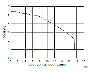
TA = 25° C; VCC = 3.3V Figure 1. Driver VOH vs Load Current
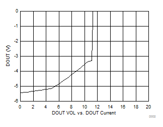
 Figure 2. Driver VOL vs Load Current