JAJSSO4 December   2023 MCT8314Z

ADVANCE INFORMATION  

  1.   1
  2. 特長
  3. アプリケーション
  4. 概要
  5. Device Comparison Table
  6. Pin Configuration and Functions
  7. Specifications
    1. 6.1 Absolute Maximum Ratings
    2. 6.2 ESD Ratings
    3. 6.3 Recommended Operating Conditions
    4. 6.4 Thermal Information
    5. 6.5 Electrical Characteristics
    6. 6.6 SPI Timing Requirements
    7. 6.7 SPI Secondary Device Mode Timings
  8. Detailed Description
    1. 7.1 Overview
    2. 7.2 Functional Block Diagram
    3. 7.3 Feature Description
      1. 7.3.1  Output Stage
      2. 7.3.2  PWM Control Mode (1x PWM Mode)
        1. 7.3.2.1 Analog Hall Input Configuration
        2. 7.3.2.2 Digital Hall Input Configuration
        3. 7.3.2.3 Asynchronous Modulation
        4. 7.3.2.4 Synchronous Modulation
        5. 7.3.2.5 Motor Operation
      3. 7.3.3  Device Interface Modes
        1. 7.3.3.1 Serial Peripheral Interface (SPI)
        2. 7.3.3.2 Hardware Interface
      4. 7.3.4  AVDD Linear Voltage Regulator
      5. 7.3.5  Charge Pump
      6. 7.3.6  Slew Rate
      7. 7.3.7  Cross Conduction (Dead Time)
      8. 7.3.8  Propagation Delay
      9. 7.3.9  Pin Diagrams
        1. 7.3.9.1 Logic Level Input Pin (Internal Pulldown)
        2. 7.3.9.2 Logic Level Input Pin (Internal Pullup)
        3. 7.3.9.3 Open Drain Pin
        4. 7.3.9.4 Push Pull Pin
        5. 7.3.9.5 Seven Level Input Pin
      10. 7.3.10 Automatic Synchronous Rectification Mode (ASR Mode)
      11. 7.3.11 Cycle-by-Cycle Current Limit
        1. 7.3.11.1 Cycle by Cycle Current Limit with 100% Duty Cycle Input
      12. 7.3.12 Hall Comparators (Analog Hall Inputs)
      13. 7.3.13 Advance Angle
      14. 7.3.14 FG Signal
      15. 7.3.15 Protections
        1. 7.3.15.1 VM Supply Undervoltage Lockout (NPOR)
        2. 7.3.15.2 AVDD Undervoltage Lockout (AVDD_UV)
        3. 7.3.15.3 VCP Charge Pump Undervoltage Lockout (CPUV)
        4. 7.3.15.4 Overvoltage Protections (OVP)
        5. 7.3.15.5 Overcurrent Protection (OCP)
          1. 7.3.15.5.1 OCP Latched Shutdown (OCP_MODE = 00b or MCT8314ZH)
          2. 7.3.15.5.2 OCP Automatic Retry (OCP_MODE = 01b)
          3. 7.3.15.5.3 OCP Report Only (OCP_MODE = 10b)
          4. 7.3.15.5.4 OCP Disabled (OCP_MODE = 11b)
        6. 7.3.15.6 Motor Lock (MTR_LOCK)
          1. 7.3.15.6.1 MTR_LOCK Latched Shutdown (MTR_LOCK_MODE = 00b)
          2. 7.3.15.6.2 MTR_LOCK Automatic Retry (MTR_LOCK_MODE = 01b or MCT8314ZH)
          3. 7.3.15.6.3 MTR_LOCK Report Only (MTR_LOCK_MODE= 10b)
          4. 7.3.15.6.4 MTR_LOCK Disabled (MTR_LOCK_MODE = 11b)
        7. 7.3.15.7 Thermal Warning (OTW)
        8. 7.3.15.8 Thermal Shutdown (OTS)
    4. 7.4 Device Functional Modes
      1. 7.4.1 Functional Modes
        1. 7.4.1.1 Sleep Mode
        2. 7.4.1.2 Operating Mode
        3. 7.4.1.3 Fault Reset (CLR_FLT or nSLEEP Reset Pulse)
    5. 7.5 SPI Communication
      1. 7.5.1 Programming
        1. 7.5.1.1 SPI Format
    6. 7.6 Register Map
      1. 7.6.1 STATUS Registers
      2. 7.6.2 CONTROL Registers
  9. Application and Implementation
    1. 8.1 Application Information
    2. 8.2 Hall Sensor Configuration and Connection
      1. 8.2.1 Typical Configuration
      2. 8.2.2 Open Drain Configuration
      3. 8.2.3 Series Configuration
      4. 8.2.4 Parallel Configuration
    3. 8.3 Typical Applications
      1. 8.3.1 Three-Phase Brushless-DC Motor Control With Current Limit
        1. 8.3.1.1 Detailed Design Procedure
          1. 8.3.1.1.1 Motor Voltage
          2. 8.3.1.1.2 Using Automatic Synchronous Rectification Mode (ASR Mode)
          3. 8.3.1.1.3 Power Dissipation and Junction Temperature Losses
  10. Power Supply Recommendations
    1. 9.1 Bulk Capacitance
  11. 10Layout
    1. 10.1 Layout Guidelines
    2. 10.2 Layout Example
    3. 10.3 Thermal Considerations
      1. 10.3.1 Power Dissipation
  12. 11Device and Documentation Support
    1. 11.1 Documentation Support
      1. 11.1.1 Related Documentation
    2. 11.2 サポート・リソース
    3. 11.3 Trademarks
    4. 11.4 静電気放電に関する注意事項
    5. 11.5 用語集
  13. 12Revision History
  14. 13Mechanical, Packaging, and Orderable Information
    1. 13.1 Package Option Addendum
    2. 13.2 Tape and Reel Information

パッケージ・オプション

メカニカル・データ(パッケージ|ピン)
サーマルパッド・メカニカル・データ
発注情報
OCP Latched Shutdown (OCP_MODE = 00b or MCT8314ZH)

After a OCP event in this mode, all MOSFETs are disabled and the nFAULT pin is driven low. The FAULT, OCP, and corresponding FET's OCP bits are latched high in the SPI registers. Normal operation starts again (driver operation and the nFAULT pin is released) when the OCP condition clears and a clear faults command is issued either through the CLR_FLT bit or an nSLEEP reset pulse (tRST).
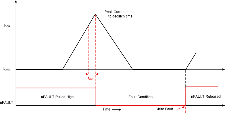
GUID-3AFC6F7D-D8D0-466D-B17B-E786F5278098-low.gifFigure 7-32 Overcurrent Protection - Latched Shutdown Mode