JAJSG95A May 2014 – September 2018 MSP430F6745A , MSP430F6746A , MSP430F6747A , MSP430F6748A , MSP430F6749A , MSP430F6765A , MSP430F6766A , MSP430F6767A , MSP430F6768A , MSP430F6769A , MSP430F6775A , MSP430F6776A , MSP430F6777A , MSP430F6778A , MSP430F6779A
PRODUCTION DATA.
- 1デバイスの概要
- 2改訂履歴
- 3Device Comparison
- 4Terminal Configuration and Functions
-
5Specifications
- 5.1 Absolute Maximum Ratings
- 5.2 ESD Ratings
- 5.3 Recommended Operating Conditions
- 5.4 Active Mode Supply Current Into VCC Excluding External Current
- 5.5 Low-Power Mode Supply Currents (Into VCC) Excluding External Current
- 5.6 Low-Power Mode With LCD Supply Currents (Into VCC) Excluding External Current
- 5.7 Thermal Resistance Characteristics
- 5.8 Timing and Switching Characteristics
- 5.9
Digital I/Os
- Table 5-6 Schmitt-Trigger Inputs – General-Purpose I/O
- Table 5-7 Inputs – Ports P1 and P2
- Table 5-8 Leakage Current – General-Purpose I/O
- Table 5-9 Outputs – General-Purpose I/O (Full Drive Strength)
- Table 5-10 Outputs – General-Purpose I/O (Reduced Drive Strength)
- Table 5-11 Output Frequency – General-Purpose I/O
- 5.9.1 Typical Characteristics – Outputs, Reduced Drive Strength (PxDS.y = 0)
- 5.9.2 Typical Characteristics – Outputs, Full Drive Strength (PxDS.y = 1)
- 5.10 Power-Management Module (PMM)
- 5.11
Auxiliary Supplies
- Table 5-18 Auxiliary Supplies, Recommended Operating Conditions
- Table 5-19 Auxiliary Supplies, AUXVCC3 (Backup Subsystem) Currents
- Table 5-20 Auxiliary Supplies, Auxiliary Supply Monitor
- Table 5-21 Auxiliary Supplies, Switch ON-Resistance
- Table 5-22 Auxiliary Supplies, Switching Time
- Table 5-23 Auxiliary Supplies, Switch Leakage
- Table 5-24 Auxiliary Supplies, Auxiliary Supplies to ADC10_A
- Table 5-25 Auxiliary Supplies, Charge Limiting Resistor
- 5.12 Timer_A
- 5.13 eUSCI
- 5.14 RTC Tamper Detect Pin
- 5.15 LCD_C
- 5.16
SD24_B
- Table 5-39 SD24_B, Power Supply and Operating Conditions
- Table 5-40 SD24_B, Analog Inputs
- Table 5-41 SD24_B, Supply Currents
- Table 5-42 SD24_B, Performance
- Table 5-43 SD24_B, AC Performance
- Table 5-44 SD24_B, AC Performance
- Table 5-45 SD24_B, AC Performance
- Table 5-46 SD24_B External Reference Input
- 5.17 ADC10_A
- 5.18 REF
- 5.19 Comparator_B
- 5.20 Flash
- 5.21 Emulation and Debug
-
6Detailed Description
- 6.1 Overview
- 6.2 Functional Block Diagrams
- 6.3 CPU (Link to User's Guide)
- 6.4 Instruction Set
- 6.5 Operating Modes
- 6.6 Interrupt Vector Addresses
- 6.7 Special Function Registers (SFRs)
- 6.8 Bootloader (BSL)
- 6.9 JTAG Operation
- 6.10 Memory
- 6.11
Peripherals
- 6.11.1 Oscillator and System Clock (Link to User's Guide)
- 6.11.2 Power-Management Module (PMM) (Link to User's Guide)
- 6.11.3 Auxiliary-Supply System (Link to User's Guide)
- 6.11.4 Backup Subsystem
- 6.11.5 Digital I/O (Link to User's Guide)
- 6.11.6 Port Mapping Controller (Link to User's Guide)
- 6.11.7 System Module (SYS) (Link to User's Guide)
- 6.11.8 Watchdog Timer (WDT_A) (Link to User's Guide)
- 6.11.9 DMA Controller (Link to User's Guide)
- 6.11.10 CRC16 (Link to User's Guide)
- 6.11.11 Hardware Multiplier (Link to User's Guide)
- 6.11.12 AES128 Accelerator (Link to User's Guide)
- 6.11.13 Enhanced Universal Serial Communication Interface (eUSCI) (Links to User's Guide: UART Mode, SPI Mode, I2C Mode)
- 6.11.14 ADC10_A (Link to User's Guide)
- 6.11.15 SD24_B (Link to User's Guide)
- 6.11.16 TA0 (Link to User's Guide)
- 6.11.17 TA1 (Link to User's Guide)
- 6.11.18 TA2 (Link to User's Guide)
- 6.11.19 TA3 (Link to User's Guide)
- 6.11.20 SD24_B Triggers
- 6.11.21 ADC10_A Triggers
- 6.11.22 Real-Time Clock (RTC_C) (Link to User's Guide)
- 6.11.23 Reference (REF) Module Voltage Reference (Link to User's Guide)
- 6.11.24 LCD_C (Link to User's Guide)
- 6.11.25 Comparator_B (Link to User's Guide)
- 6.11.26 Embedded Emulation Module (EEM) (Link to User's Guide)
- 6.11.27 Peripheral File Map
- 6.12
Input/Output Diagrams
- 6.12.1 Port P1 (P1.0 to P1.3) Input/Output With Schmitt Trigger (PEU Package Only)
- 6.12.2 Port P1 (P1.0 to P1.3) Input/Output With Schmitt Trigger (PZ Package Only)
- 6.12.3 Port P1 (P1.4 and P1.5) Input/Output With Schmitt Trigger
- 6.12.4 Port P1 (P1.6 and P1.7) Input/Output With Schmitt Trigger
- 6.12.5 Port P2 (P2.0 to P2.7) Input/Output With Schmitt Trigger (PEU Package Only)
- 6.12.6 Port P2 (P2.0 to P2.3) Input/Output With Schmitt Trigger (PZ Package Only)
- 6.12.7 Port P2 (P2.4 to P2.6) Input/Output With Schmitt Trigger (PZ Package Only)
- 6.12.8 Port P2 (P2.7) Input/Output With Schmitt Trigger (PZ Package Only)
- 6.12.9 Ports P3 (P3.0 to P3.7) Input/Output With Schmitt Trigger (PEU Package Only)
- 6.12.10 Ports P3 (P3.0) Input/Output With Schmitt Trigger (PZ Package Only)
- 6.12.11 Ports P3 (P3.1 to P3.7) Input/Output With Schmitt Trigger (PZ Package Only)
- 6.12.12 Port P4 (P4.0 to P4.7) Input/Output With Schmitt Trigger (PEU Package Only)
- 6.12.13 Port P4 (P4.0 to P4.7) Input/Output With Schmitt Trigger (PZ Package Only)
- 6.12.14 Port P5 (P5.0 to P5.3) Input/Output With Schmitt Trigger (PEU Package Only)
- 6.12.15 Port P5 (P5.4 to P5.6) Input/Output With Schmitt Trigger (PEU Package Only)
- 6.12.16 Port P5 (P5.7) Input/Output With Schmitt Trigger (PEU Package Only)
- 6.12.17 Port P5 (P5.0 to P5.7) Input/Output With Schmitt Trigger (PZ Package Only)
- 6.12.18 Port P6 (P6.0) Input/Output With Schmitt Trigger (PEU Package Only)
- 6.12.19 Port P6 (P6.1 to P6.3) Input/Output With Schmitt Trigger (PEU Package Only)
- 6.12.20 Port P6 (P6.4 to P6.7) Input/Output With Schmitt Trigger (PEU Package Only)
- 6.12.21 Port P6 (P6.0 to P6.7) Input/Output With Schmitt Trigger (PZ Package Only)
- 6.12.22 Port P7 (P7.0 to P7.7) Input/Output With Schmitt Trigger (PEU Package Only)
- 6.12.23 Port P7 (P7.0 to P7.7) Input/Output With Schmitt Trigger (PZ Package Only)
- 6.12.24 Port P8 (P8.0 to P8.7) Input/Output With Schmitt Trigger (PEU Package Only)
- 6.12.25 Port P8 (P8.0) Input/Output With Schmitt Trigger (PZ Package Only)
- 6.12.26 Port P8 (P8.1) Input/Output With Schmitt Trigger (PZ Package Only)
- 6.12.27 Port P9 (P9.0 to P9.7) Input/Output With Schmitt Trigger (PEU Package Only)
- 6.12.28 Port P10 (P10.0 to P10.7) Input/Output With Schmitt Trigger (PEU Package Only)
- 6.12.29 Port P11 (P11.0) Input/Output With Schmitt Trigger (PEU Package Only)
- 6.12.30 Port P11 (P11.1) Input/Output With Schmitt Trigger (PEU Package Only)
- 6.12.31 Port P11 (P11.2 and P11.3) Input/Output With Schmitt Trigger (PEU Package Only)
- 6.12.32 Port P11 (P11.4 and P11.5) Input/Output With Schmitt Trigger (PEU Package Only)
- 6.12.33 Port PJ (PJ.0) JTAG Pin TDO, Input/Output With Schmitt Trigger or Output
- 6.12.34 Port PJ (PJ.0 to PJ.3) JTAG Pins TMS, TCK, TDI/TCLK, Input/Output With Schmitt Trigger or Output
- 6.13 Device Descriptors (TLV)
- 6.14 Identification
- 7Applications, Implementation, and Layout
- 8デバイスおよびドキュメントのサポート
- 9メカニカル、パッケージ、および注文情報
パッケージ・オプション
メカニカル・データ(パッケージ|ピン)
サーマルパッド・メカニカル・データ
発注情報
4.1 Pin Diagrams
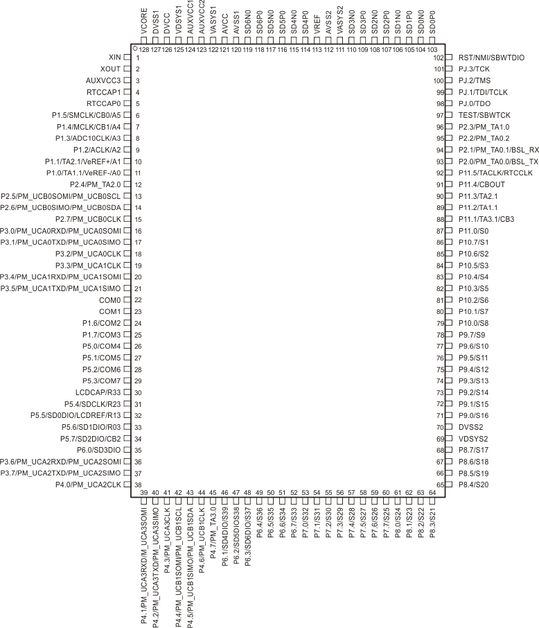
Figure 4-1 shows the pinout for the 128-pin PEU package. Table 4-1 summarizes the differences in the pinout among the device variants.

A. The secondary digital functions on Ports P2, P3, and P4 are fully mappable. This pinout shows only the default mapping. See Section 6.11.6 for details.
B. The pair of pins VDSYS1 and VDSYS2, VASYS1 and VASYS2 must be connected externally on board for proper device operation.
C. CAUTION: The LCDCAP/R33 pin must be connected to DVSS if it is not used.
Figure 4-1 128-Pin PEU Package (Top View) Table 4-1 Pinout Differences for PEU Package, F677xA, F676xA, and F674xA
| PIN NUMBER | PIN NAME | ||
|---|---|---|---|
| MSP430F677xAIPEU | MSP430F676xAIPEU | MSP430F674xAIPEU | |
| 46 | P6.1/SD4DIO/S39 | P6.1/SD4DIO/S39 | P6.1/S39 |
| 47 | P6.2/SD5DIO/S38 | P6.2/SD5DIO/S38 | P6.2/S38 |
| 48 | P6.3/SD6DIO/S37 | P6.3/S37 | P6.3/S37 |
| 113 | VREF | VREF | VREF |
| 114 | SD4P0 | SD4P0 | NC |
| 115 | SD4N0 | SD4N0 | NC |
| 116 | SD5P0 | SD5P0 | NC |
| 117 | SD5N0 | SD5NO | NC |
| 118 | SD6P0 | NC | NC |
| 119 | SD6N0 | NC | NC |
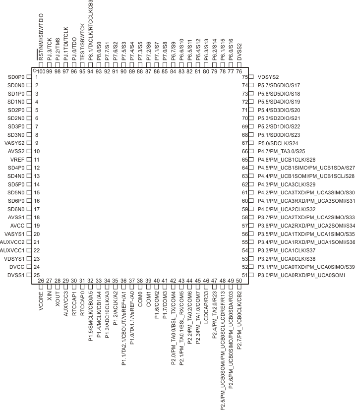
Figure 4-2 shows the pinout for the 100-pin PZ package. Table 4-2 summarizes the differences in the pinout among the device variants.

A. The secondary digital functions on Ports P2, P3, and P4 are fully mappable. This pinout shows only the default mapping. See Section 6.11.6 for details.
B. The pair of pins VDSYS1 and VDSYS2, VASYS1 and VASYS2 must be connected externally on board for proper device operation.
C. CAUTION: The LCDCAP/R33 pin must be connected to DVSS if it is not used.
Figure 4-2 100-Pin PZ Package (Top View) Table 4-2 Pinout Differences for PZ Package, F677xA, F676xA, and F674xA
| PIN NUMBER | PIN NAME | ||
|---|---|---|---|
| MSP430F677xAIPZ | MSP430F676xAIPZ | MSP430F674xAIPZ | |
| 11 | VREF | VREF | VREF |
| 12 | SD4P0 | SD4P0 | NC |
| 13 | SD4N0 | SD4N0 | NC |
| 14 | SD5P0 | SD5P0 | NC |
| 15 | SD5N0 | SD5NO | NC |
| 16 | SD6P0 | NC | NC |
| 17 | SD6N0 | NC | NC |
| 72 | P5.5/SD4DIO/S19 | P5.5/SD4DIO/S19 | P5.5/S19 |
| 73 | P5.6/SD5DIO/S18 | P5.6/SD5DIO/S18 | P5.6/S18 |
| 74 | P5.7/SD6DIO/S17 | P5.7/S17 | P5.7/S17 |