JAJSG09F October 2015 – December 2019 MSP430FR2433
PRODUCTION DATA.
- 1デバイスの概要
- 2改訂履歴
- 3Device Comparison
- 4Terminal Configuration and Functions
-
5Specifications
- 5.1 Absolute Maximum Ratings
- 5.2 ESD Ratings
- 5.3 Recommended Operating Conditions
- 5.4 Active Mode Supply Current Into VCC Excluding External Current
- 5.5 Active Mode Supply Current Per MHz
- 5.6 Low-Power Mode LPM0 Supply Currents Into VCC Excluding External Current
- 5.7 Low-Power Mode (LPM3 and LPM4) Supply Currents (Into VCC) Excluding External Current
- 5.8 Low-Power Mode LPMx.5 Supply Currents (Into VCC) Excluding External Current
- 5.9 Typical Characteristics - Low-Power Mode Supply Currents
- Table 5-1 Typical Characteristics – Current Consumption Per Module
- 5.10 Thermal Resistance Characteristics
- 5.11 Timing and Switching Characteristics
-
6Detailed Description
- 6.1 Overview
- 6.2 CPU
- 6.3 Operating Modes
- 6.4 Interrupt Vector Addresses
- 6.5 Bootloader (BSL)
- 6.6 JTAG Standard Interface
- 6.7 Spy-Bi-Wire Interface (SBW)
- 6.8 FRAM
- 6.9 Memory Protection
- 6.10
Peripherals
- 6.10.1 Power-Management Module (PMM)
- 6.10.2 Clock System (CS) and Clock Distribution
- 6.10.3 General-Purpose Input/Output Port (I/O)
- 6.10.4 Watchdog Timer (WDT)
- 6.10.5 System (SYS) Module
- 6.10.6 Cyclic Redundancy Check (CRC)
- 6.10.7 Enhanced Universal Serial Communication Interface (eUSCI_A0, eUSCI_B0)
- 6.10.8 Timers (Timer0_A3, Timer1_A3, Timer2_A2 and Timer3_A2)
- 6.10.9 Hardware Multiplier (MPY)
- 6.10.10 Backup Memory (BAKMEM)
- 6.10.11 Real-Time Clock (RTC)
- 6.10.12 10-Bit Analog-to-Digital Converter (ADC)
- 6.10.13 Embedded Emulation Module (EEM)
- 6.11 Input/Output Diagrams
- 6.12 Device Descriptors
- 6.13 Memory
- 6.14 Identification
- 7Applications, Implementation, and Layout
- 8デバイスおよびドキュメントのサポート
- 9メカニカル、パッケージ、および注文情報
パッケージ・オプション
メカニカル・データ(パッケージ|ピン)
サーマルパッド・メカニカル・データ
- RGE|24
発注情報
Table 5-17 eUSCI (SPI Master Mode)
over recommended ranges of supply voltage and operating free-air temperature (unless otherwise noted)(1)| PARAMETER | TEST CONDITIONS | VCC | MIN | MAX | UNIT | |
|---|---|---|---|---|---|---|
| tSTE,LEAD | STE lead time, STE active to clock | UCSTEM = 0, UCMODEx = 01 or 10 | 1 | UCxCLK cycles | ||
| UCSTEM = 1, UCMODEx = 01 or 10 | ||||||
| tSTE,LAG | STE lag time, last clock to STE inactive | UCSTEM = 0, UCMODEx = 01 or 10 | 1 | UCxCLK cycles | ||
| UCSTEM = 1, UCMODEx = 01 or 10 | ||||||
| tSU,MI | SOMI input data setup time | 2 V | 45 | ns | ||
| 3 V | 35 | |||||
| tHD,MI | SOMI input data hold time | 2 V | 0 | ns | ||
| 3 V | 0 | |||||
| tVALID,MO | SIMO output data valid time(2) | UCLK edge to SIMO valid,
CL = 20 pF |
2 V | 20 | ns | |
| 3 V | 20 | |||||
| tHD,MO | SIMO output data hold time(3) | CL = 20 pF | 2 V | 0 | ns | |
| 3 V | 0 | |||||
(1) fUCxCLK = 1 / 2tLO/HI with tLO/HI = max(tVALID,MO(eUSCI) + tSU,SI(Slave), tSU,MI(eUSCI) + tVALID,SO(Slave))
For the slave parameters tSU,SI(Slave) and tVALID,SO(Slave), see the SPI parameters of the attached slave.
For the slave parameters tSU,SI(Slave) and tVALID,SO(Slave), see the SPI parameters of the attached slave.
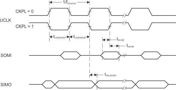
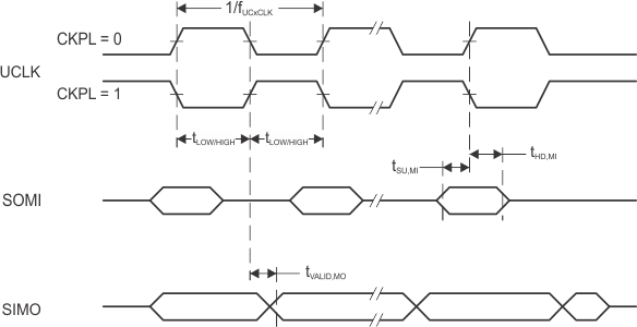
(2) Specifies the time to drive the next valid data to the SIMO output after the output changing UCLK clock edge. See the timing diagrams in Figure 5-12 and Figure 5-13.
(3) Specifies how long data on the SIMO output is valid after the output changing UCLK clock edge. Negative values indicate that the data on the SIMO output can become invalid before the output changing clock edge observed on UCLK. See the timing diagrams in Figure 5-12 and Figure 5-13.
 Figure 5-12 SPI Master Mode, CKPH = 0
  Figure 5-13 SPI Master Mode, CKPH = 1
 Table 5-18 lists the characteristics of the eUSCI in SPI slave mode.