JAJSH22C March   2019  – September 2021 MSP430FR2475 , MSP430FR2476

PRODUCTION DATA  

  1. 特長
  2. アプリケーション
  3. 概要
  4. 機能ブロック図
  5. Revision History
  6. Device Comparison
    1. 6.1 Related Products
  7. Terminal Configuration and Functions
    1. 7.1 Pin Diagrams
    2. 7.2 Pin Attributes
    3. 7.3 Signal Descriptions
    4. 7.4 Pin Multiplexing
    5. 7.5 Buffer Types
    6. 7.6 Connection of Unused Pins
  8. Specifications
    1. 8.1  Absolute Maximum Ratings
    2. 8.2  ESD Ratings
    3. 8.3  Recommended Operating Conditions
    4. 8.4  Active Mode Supply Current Into VCC Excluding External Current
    5. 8.5  Active Mode Supply Current Per MHz
    6. 8.6  Low-Power Mode LPM0 Supply Currents Into VCC Excluding External Current
    7. 8.7  Low-Power Mode (LPM3, LPM4) Supply Currents (Into VCC) Excluding External Current
    8. 8.8  Low-Power Mode LPMx.5 Supply Currents (Into VCC) Excluding External Current
    9. 8.9  Typical Characteristics – Low-Power Mode Supply Currents
    10. 8.10 Current Consumption Per Module
    11. 8.11 Thermal Resistance Characteristics
    12. 8.12 Timing and Switching Characteristics
      1. 8.12.1  Power Supply Sequencing
        1. 8.12.1.1 PMM, SVS and BOR
      2. 8.12.2  Reset Timing
        1. 8.12.2.1 Wake-up Times From Low-Power Modes and Reset
      3. 8.12.3  Clock Specifications
        1. 8.12.3.1 XT1 Crystal Oscillator (Low Frequency)
        2. 8.12.3.2 DCO FLL, Frequency
        3. 8.12.3.3 DCO Frequency
        4. 8.12.3.4 REFO
        5. 8.12.3.5 Internal Very-Low-Power Low-Frequency Oscillator (VLO)
        6. 8.12.3.6 Module Oscillator (MODOSC)
      4. 8.12.4  Digital I/Os
        1. 8.12.4.1 Digital Inputs
        2. 8.12.4.2 Digital Outputs
        3. 8.12.4.3 Typical Characteristics – Outputs at 3 V and 2 V
      5. 8.12.5  Internal Shared Reference
        1. 8.12.5.1 Internal Reference Characteristics
      6. 8.12.6  Timer_A and Timer_B
        1. 8.12.6.1 Timer_A
        2. 8.12.6.2 Timer_B
      7. 8.12.7  eUSCI
        1. 8.12.7.1 eUSCI (UART Mode) Clock Frequency
        2. 8.12.7.2 eUSCI (UART Mode) Timing Characteristics
        3. 8.12.7.3 eUSCI (SPI Master Mode) Clock Frequency
        4. 8.12.7.4 eUSCI (SPI Master Mode)
        5. 8.12.7.5 eUSCI (SPI Slave Mode)
        6. 8.12.7.6 eUSCI (I2C Mode)
      8. 8.12.8  ADC
        1. 8.12.8.1 ADC, Power Supply and Input Range Conditions
        2. 8.12.8.2 ADC, Timing Parameters
        3. 8.12.8.3 ADC, Linearity Parameters
      9. 8.12.9  Enhanced Comparator (eCOMP)
        1. 8.12.9.1 eCOMP0 Characteristics
      10. 8.12.10 FRAM
        1. 8.12.10.1 FRAM Characteristics
      11. 8.12.11 Debug and Emulation
        1. 8.12.11.1 JTAG, 4-Wire and Spy-Bi-Wire Interface
  9. Detailed Description
    1. 9.1  Overview
    2. 9.2  CPU
    3. 9.3  Operating Modes
    4. 9.4  Interrupt Vector Addresses
    5. 9.5  Bootloader (BSL)
    6. 9.6  JTAG Standard Interface
    7. 9.7  Spy-Bi-Wire Interface (SBW)
    8. 9.8  FRAM
    9. 9.9  Memory Protection
    10. 9.10 Peripherals
      1. 9.10.1  Power-Management Module (PMM)
      2. 9.10.2  Clock System (CS) and Clock Distribution
      3. 9.10.3  General-Purpose Input/Output Port (I/O)
      4. 9.10.4  Watchdog Timer (WDT)
      5. 9.10.5  System (SYS) Module
      6. 9.10.6  Cyclic Redundancy Check (CRC)
      7. 9.10.7  Enhanced Universal Serial Communication Interface (eUSCI_A0, eUSCI_B0)
      8. 9.10.8  Timers (TA0, TA1, TA2, TA3 and TB0)
      9. 9.10.9  Hardware Multiplier (MPY)
      10. 9.10.10 Backup Memory (BAKMEM)
      11. 9.10.11 Real-Time Clock (RTC)
      12. 9.10.12 12-Bit Analog-to-Digital Converter (ADC)
      13. 9.10.13 eCOMP0
      14. 9.10.14 Embedded Emulation Module (EEM)
    11. 9.11 Input/Output Diagrams
      1. 9.11.1 Port P1 (P1.0 to P1.7) Input/Output With Schmitt Trigger
      2. 9.11.2 Port P2 (P2.0 to P2.7) Input/Output With Schmitt Trigger
      3. 9.11.3 Port P3 (P3.0 to P3.7) Input/Output With Schmitt Trigger
      4. 9.11.4 Port P4 (P4.0 to P4.7) Input/Output With Schmitt Trigger
      5. 9.11.5 Port P5 (P5.0 to P5.7) Input/Output With Schmitt Trigger
      6. 9.11.6 Port P6 (P6.0 to P6.2) Input/Output With Schmitt Trigger
    12. 9.12 Device Descriptors
    13. 9.13 Memory
      1. 9.13.1 Memory Organization
      2. 9.13.2 Peripheral File Map
    14. 9.14 Identification
      1. 9.14.1 Revision Identification
      2. 9.14.2 Device Identification
      3. 9.14.3 JTAG Identification
  10. 10Applications, Implementation, and Layout
    1. 10.1 Device Connection and Layout Fundamentals
      1. 10.1.1 Power Supply Decoupling and Bulk Capacitors
      2. 10.1.2 External Oscillator
      3. 10.1.3 JTAG
      4. 10.1.4 Reset
      5. 10.1.5 Unused Pins
      6. 10.1.6 General Layout Recommendations
      7. 10.1.7 Do's and Don'ts
    2. 10.2 Peripheral- and Interface-Specific Design Information
      1. 10.2.1 ADC Peripheral
        1. 10.2.1.1 Partial Schematic
        2. 10.2.1.2 Design Requirements
        3. 10.2.1.3 Layout Guidelines
  11. 11Device and Documentation Support
    1. 11.1 Getting Started and Next Steps
    2. 11.2 Device Nomenclature
    3. 11.3 Tools and Software
    4. 11.4 Documentation Support
    5. 11.5 サポート・リソース
    6. 11.6 Trademarks
    7. 11.7 Electrostatic Discharge Caution
    8. 11.8 Export Control Notice
    9. 11.9 Glossary
  12. 12Mechanical, Packaging, and Orderable Information

パッケージ・オプション

メカニカル・データ(パッケージ|ピン)
サーマルパッド・メカニカル・データ
発注情報

JTAG

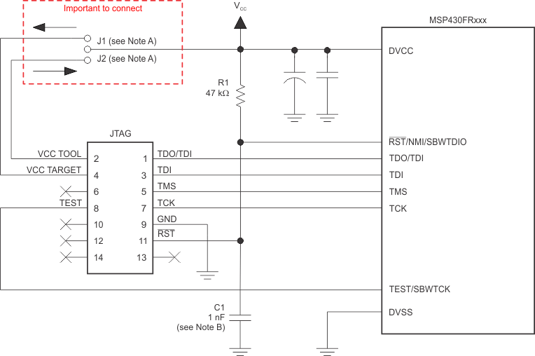
With the proper connections, the debugger and a hardware JTAG interface (such as the MSP-FET or MSP-FET430UIF) can be used to program and debug code on the target board. In addition, the connections also support the MSP-GANG production programmers, thus providing an easy way to program prototype boards, if desired. Figure 10-3 shows the connections between the 14-pin JTAG connector and the target device required to support in-system programming and debugging for 4-wire JTAG communication. Figure 10-4 shows the connections for 2-wire JTAG mode (Spy-Bi-Wire).

The connections for the MSP-FET and MSP-FET430UIF interface modules and the MSP-GANG are identical. Both can supply VCC to the target board (through pin 2). In addition, the MSP-FET and MSP-FET430UIF interface modules and MSP-GANG have a VCC sense feature that, if used, requires an alternate connection (pin 4 instead of pin 2). The VCC sense feature detects the local VCC present on the target board (that is, a battery or other local power supply) and adjusts the output signals accordingly. Figure 10-3 and Figure 10-4 show a jumper block that supports both scenarios of supplying VCC to the target board. If this flexibility is not required, the desired VCC connections may be hard-wired to eliminate the jumper block. Pins 2 and 4 must not be connected at the same time.

For additional design information regarding the JTAG interface, see the MSP430 Hardware Tools User's Guide.
GUID-D8C0F8E3-2A72-4979-853D-664755C4542B-low.gif
If a local target power supply is used, make connection J1. If power from the debug or programming adapter is used, make connection J2.
The upper limit for C1 is 1.1 nF when using current TI tools.
Figure 10-3 Signal Connections for 4-Wire JTAG Communication
GUID-04B4C53C-2B8A-4CE2-9B99-F071DFA3E241-low.gif
Make connection J1 if a local target power supply is used, or make connection J2 if the target is powered from the debug or programming adapter.
The device RST/NMI/SBWTDIO pin is used in 2-wire mode for bidirectional communication with the device during JTAG access, and any capacitance that is attached to this signal may affect the ability to establish a connection with the device. The upper limit for C1 is 1.1 nF when using current TI tools.
Figure 10-4 Signal Connections for 2-Wire JTAG Communication (Spy-Bi-Wire)