JAJSG14E May 2014 – August 2018 MSP430FR5847 , MSP430FR58471 , MSP430FR5848 , MSP430FR5849 , MSP430FR5857 , MSP430FR5858 , MSP430FR5859 , MSP430FR5867 , MSP430FR58671 , MSP430FR5868 , MSP430FR5869
PRODUCTION DATA.
- 1デバイスの概要
- 2改訂履歴
- 3Device Comparison
- 4Terminal Configuration and Functions
-
5Specifications
- 5.1 Absolute Maximum Ratings
- 5.2 ESD Ratings
- 5.3 Recommended Operating Conditions
- 5.4 Active Mode Supply Current Into VCC Excluding External Current
- 5.5 Typical Characteristics – Active Mode Supply Currents
- 5.6 Low-Power Mode (LPM0, LPM1) Supply Currents Into VCC Excluding External Current
- 5.7 Low-Power Mode (LPM2, LPM3, LPM4) Supply Currents (Into VCC) Excluding External Current
- 5.8 Low-Power Mode (LPM3.5, LPM4.5) Supply Currents (Into VCC) Excluding External Current
- 5.9 Typical Characteristics, Low-Power Mode Supply Currents
- 5.10 Typical Characteristics, Current Consumption per Module
- 5.11 Thermal Resistance Characteristics
- 5.12
Timing and Switching Characteristics
- 5.12.1 Power Supply Sequencing
- 5.12.2 Reset Timing
- 5.12.3 Clock Specifications
- 5.12.4 Wake-up Characteristics
- 5.12.5 Digital I/Os
- 5.12.6 Timer_A and Timer_B
- 5.12.7 eUSCI
- 5.12.8
ADC
- Table 5-22 12-Bit ADC, Power Supply and Input Range Conditions
- Table 5-23 12-Bit ADC, Timing Parameters
- Table 5-24 12-Bit ADC, Linearity Parameters With External Reference
- Table 5-25 12-Bit ADC, Dynamic Performance for Differential Inputs With External Reference
- Table 5-26 12-Bit ADC, Dynamic Performance for Differential Inputs With Internal Reference
- Table 5-27 12-Bit ADC, Dynamic Performance for Single-Ended Inputs With External Reference
- Table 5-28 12-Bit ADC, Dynamic Performance for Single-Ended Inputs With Internal Reference
- Table 5-29 12-Bit ADC, Dynamic Performance With 32.768-kHz Clock
- Table 5-30 12-Bit ADC, Temperature Sensor and Built-In V1/2
- Table 5-31 12-Bit ADC, External Reference
- 5.12.9 Reference
- 5.12.10 Comparator
- 5.12.11 FRAM
- 5.13 Emulation and Debug
-
6Detailed Description
- 6.1 Overview
- 6.2 CPU
- 6.3 Operating Modes
- 6.4 Interrupt Vector Table and Signatures
- 6.5 Memory Organization
- 6.6 Bootloader (BSL)
- 6.7 JTAG Operation
- 6.8 FRAM
- 6.9 Memory Protection Unit Including IP Encapsulation
- 6.10
Peripherals
- 6.10.1 Digital I/O
- 6.10.2 Oscillator and Clock System (CS)
- 6.10.3 Power-Management Module (PMM)
- 6.10.4 Hardware Multiplier (MPY)
- 6.10.5 Real-Time Clock (RTC_B) (Only MSP430FR586x and MSP430FR584x)
- 6.10.6 Watchdog Timer (WDT_A)
- 6.10.7 System Module (SYS)
- 6.10.8 DMA Controller
- 6.10.9 Enhanced Universal Serial Communication Interface (eUSCI)
- 6.10.10 TA0, TA1
- 6.10.11 TA2, TA3
- 6.10.12 TB0
- 6.10.13 ADC12_B
- 6.10.14 Comparator_E
- 6.10.15 CRC16
- 6.10.16 True Random Seed
- 6.10.17 Shared Reference (REF)
- 6.10.18 Embedded Emulation
- 6.10.19 Peripheral File Map
- 6.11
Input/Output Diagrams
- 6.11.1 Capacitive Touch Functionality Ports P1, P2, P3, P4, and PJ
- 6.11.2 Port P1 (P1.0 to P1.2) Input/Output With Schmitt Trigger
- 6.11.3 Port P1 (P1.3 to P1.5) Input/Output With Schmitt Trigger
- 6.11.4 Port P1 (P1.6 and P1.7) Input/Output With Schmitt Trigger
- 6.11.5 Port P2 (P2.0 to P2.2) Input/Output With Schmitt Trigger
- 6.11.6 Port P2 (P2.3 and P2.4) Input/Output With Schmitt Trigger
- 6.11.7 Port P2 (P2.5 and P2.6) Input/Output With Schmitt Trigger
- 6.11.8 Port P2 (P2.7) Input/Output With Schmitt Trigger
- 6.11.9 Port P3 (P3.0 to P3.3) Input/Output With Schmitt Trigger
- 6.11.10 Port P3 (P3.4 to P3.7) Input/Output With Schmitt Trigger
- 6.11.11 Port P4 (P4.0 to P4.3) Input/Output With Schmitt Trigger
- 6.11.12 Port P4 (P4.4 to P4.7) Input/Output With Schmitt Trigger
- 6.11.13 Port PJ, PJ.4 and PJ.5 Input/Output With Schmitt Trigger
- 6.11.14 Port PJ (PJ.6 and PJ.7) Input/Output With Schmitt Trigger
- 6.11.15 Port PJ (PJ.0 to PJ.3) JTAG Pins TDO, TMS, TCK, TDI/TCLK, Input/Output With Schmitt Trigger
- 6.12 Device Descriptor (TLV)
- 6.13 Identification
- 7Applications, Implementation, and Layout
- 8デバイスおよびドキュメントのサポート
- 9メカニカル、パッケージ、および注文情報
パッケージ・オプション
メカニカル・データ(パッケージ|ピン)
サーマルパッド・メカニカル・データ
- DA|38
発注情報
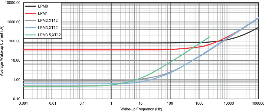
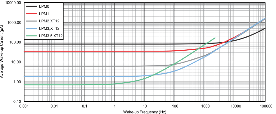
5.12.4.1 Typical Characteristics, Average LPM Currents vs Wake-up Frequency

NOTE:
The average wakeup current does not include the energy required in active mode; for example, for an interrupt service routine or to reconfigure the device.
NOTE:
The average wakeup current does not include the energy required in active mode; for example, for an interrupt service routine or to reconfigure the device.