JAJSDV8E August 2011 – January 2017 OMAP-L132
PRODUCTION DATA.
- 1デバイスの概要
- 2Revision History
-
3Device Comparison
- 3.1 Device Characteristics
- 3.2 Device Compatibility
- 3.3 ARM Subsystem
- 3.4 DSP Subsystem
- 3.5 Memory Map Summary
- 3.6 Pin Assignments
- 3.7 Pin Multiplexing Control
- 3.8
Terminal Functions
- 3.8.1 Device Reset, NMI and JTAG
- 3.8.2 High-Frequency Oscillator and PLL
- 3.8.3 Real-Time Clock and 32-kHz Oscillator
- 3.8.4 DEEPSLEEP Power Control
- 3.8.5 External Memory Interface A (EMIFA)
- 3.8.6 DDR2/mDDR Controller
- 3.8.7 Serial Peripheral Interface Modules (SPI)
- 3.8.8 Programmable Real-Time Unit (PRU)
- 3.8.9 Enhanced Capture/Auxiliary PWM Modules (eCAP0)
- 3.8.10 Enhanced Pulse Width Modulators (eHRPWM)
- 3.8.11 Boot
- 3.8.12 Universal Asynchronous Receiver/Transmitters (UART0, UART1, UART2)
- 3.8.13 Inter-Integrated Circuit Modules(I2C0, I2C1)
- 3.8.14 Timers
- 3.8.15 Multichannel Audio Serial Ports (McASP)
- 3.8.16 Multichannel Buffered Serial Ports (McBSP)
- 3.8.17 Universal Serial Bus Modules (USB0)
- 3.8.18 Ethernet Media Access Controller (EMAC)
- 3.8.19 Multimedia Card/Secure Digital (MMC/SD)
- 3.8.20 General Purpose Input Output
- 3.8.21 Reserved and No Connect
- 3.8.22 Supply and Ground
- 3.9 Unused Pin Configurations
- 4Device Configuration
-
5Specifications
- 5.1 Absolute Maximum Ratings Over Operating Junction Temperature Range (Unless Otherwise Noted)
- 5.2 Handling Ratings
- 5.3 Recommended Operating Conditions
- 5.4 Notes on Recommended Power-On Hours (POH)
- 5.5 Electrical Characteristics Over Recommended Ranges of Supply Voltage and Operating Junction Temperature (Unless Otherwise Noted)
-
6Peripheral Information and Electrical Specifications
- 6.1 Parameter Information
- 6.2 Recommended Clock and Control Signal Transition Behavior
- 6.3 Power Supplies
- 6.4 Reset
- 6.5 Crystal Oscillator or External Clock Input
- 6.6 Clock PLLs
- 6.7 Interrupts
- 6.8 Power and Sleep Controller (PSC)
- 6.9 Enhanced Direct Memory Access Controller (EDMA3)
- 6.10 External Memory Interface A (EMIFA)
- 6.11
DDR2/mDDR Memory Controller
- 6.11.1 DDR2/mDDR Memory Controller Electrical Data/Timing
- 6.11.2 DDR2/mDDR Memory Controller Register Description(s)
- 6.11.3
DDR2/mDDR Interface
- 6.11.3.1 DDR2/mDDR Interface Schematic
- 6.11.3.2 Compatible JEDEC DDR2/mDDR Devices
- 6.11.3.3 PCB Stackup
- 6.11.3.4 Placement
- 6.11.3.5 DDR2/mDDR Keep Out Region
- 6.11.3.6 Bulk Bypass Capacitors
- 6.11.3.7 High-Speed Bypass Capacitors
- 6.11.3.8 Net Classes
- 6.11.3.9 DDR2/mDDR Signal Termination
- 6.11.3.10 VREF Routing
- 6.11.3.11 DDR2/mDDR CK and ADDR_CTRL Routing
- 6.11.3.12 DDR2/mDDR Boundary Scan Limitations
- 6.12 Memory Protection Units
- 6.13 MMC / SD / SDIO (MMCSD0, MMCSD1)
- 6.14 Multichannel Audio Serial Port (McASP)
- 6.15
Multichannel Buffered Serial Port (McBSP)
- 6.15.1 McBSP Peripheral Register Description(s)
- 6.15.2
McBSP Electrical Data/Timing
- 6.15.2.1
Multichannel Buffered Serial Port (McBSP) Timing
- Table 6-52 Timing Requirements for McBSP0 [1.2V, 1.1V] (see )
- Table 6-53 Timing Requirements for McBSP0 [1.0V] (see )
- Table 6-54 Switching Characteristics for McBSP0 [1.2V, 1.1V] (see )
- Table 6-55 Switching Characteristics for McBSP0 [1.0V] (see )
- Table 6-56 Timing Requirements for McBSP1 [1.2V, 1.1V] (see )
- Table 6-57 Timing Requirements for McBSP1 [1.0V] (see )
- Table 6-58 Switching Characteristics for McBSP1 [1.2V, 1.1V] (see )
- Table 6-59 Switching Characteristics for McBSP1 [1.0V] (see )
- Table 6-60 Timing Requirements for McBSP0 FSR When GSYNC = 1 (see )
- Table 6-61 Timing Requirements for McBSP1 FSR When GSYNC = 1 (see )
- 6.15.2.1
Multichannel Buffered Serial Port (McBSP) Timing
- 6.16
Serial Peripheral Interface Ports (SPI0, SPI1)
- 6.16.1 SPI Peripheral Registers Description(s)
- 6.16.2
SPI Electrical Data/Timing
- 6.16.2.1
Serial Peripheral Interface (SPI) Timing
- Table 6-63 General Timing Requirements for SPI0 Master Modes
- Table 6-64 General Timing Requirements for SPI0 Slave Modes
- Table 6-71 General Timing Requirements for SPI1 Master Modes
- Table 6-72 General Timing Requirements for SPI1 Slave Modes
- Table 6-73 Additional SPI1 Master Timings, 4-Pin Enable Option
- Table 6-74 Additional SPI1 Master Timings, 4-Pin Chip Select Option
- 6.16.2.1
Serial Peripheral Interface (SPI) Timing
- 6.17 Inter-Integrated Circuit Serial Ports (I2C)
- 6.18 Universal Asynchronous Receiver/Transmitter (UART)
- 6.19 Universal Serial Bus OTG Controller (USB0) [USB2.0 OTG]
- 6.20 Ethernet Media Access Controller (EMAC)
- 6.21 Management Data Input/Output (MDIO)
- 6.22 Enhanced Capture (eCAP) Peripheral
- 6.23 Enhanced High-Resolution Pulse-Width Modulator (eHRPWM)
- 6.24 Timers
- 6.25 Real Time Clock (RTC)
- 6.26 General-Purpose Input/Output (GPIO)
- 6.27 Programmable Real-Time Unit Subsystem (PRUSS)
- 6.28 Emulation Logic
- 7Device and Documentation Support
- 8Mechanical Packaging and Orderable Information
パッケージ・オプション
デバイスごとのパッケージ図は、PDF版データシートをご参照ください。
メカニカル・データ(パッケージ|ピン)
- ZWT|361
サーマルパッド・メカニカル・データ
発注情報
6.11.3.4 Placement
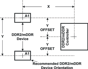
Figure 6-19 shows the required placement for the device as well as the DDR2/mDDR devices. The dimensions for Figure 6-20 are defined in Table 6-30. The placement does not restrict the side of the PCB that the devices are mounted on. The ultimate purpose of the placement is to limit the maximum trace lengths and allow for proper routing space. For single-memory DDR2/mDDR systems, the second DDR2/mDDR device is omitted from the placement.
 Figure 6-20 OMAP-L132 and DDR2/mDDR Device Placement
Table 6-30 Placement Specifications(1)(2)
| NO. | PARAMETER | MIN | MAX | UNIT |
|---|---|---|---|---|
| 1 | X | 1750 | Mils | |
| 2 | Y | 1280 | Mils | |
| 3 | Y Offset | (3) | 650 | Mils |
| 4 | Clearance from non-DDR2/mDDR signal to DDR2/mDDR Keepout Region(4) | 4 | w(5) |
(1) See Figure 6-20 for dimension definitions.
(2) Measurements from center of device to center of DDR2/mDDR device.
(3) For single memory systems it is recommended that Y Offset be as small as possible.
(4) Non-DDR2/mDDR signals allowed within DDR2/mDDR keepout region provided they are separated from DDR2/mDDR routing layers by a ground plane.
(5) w = PCB trace width as defined in Table 6-29.