JAJSGT8F June   2010  – March 2023 OPA140 , OPA2140 , OPA4140

PRODUCTION DATA  

  1.   1
  2. 特長
  3. アプリケーション
  4. 概要
  5. Revision History
  6. Pin Configuration and Functions
  7. Specifications
    1. 6.1 Absolute Maximum Ratings
    2. 6.2 ESD Ratings
    3. 6.3 Recommended Operating Conditions
    4. 6.4 Thermal Information: OPA140
    5. 6.5 Thermal Information: OPA2140
    6. 6.6 Thermal Information: OPA4140
    7. 6.7 Electrical Characteristics
    8. 6.8 Typical Characteristics
  8. Detailed Description
    1. 7.1 Overview
    2. 7.2 Functional Block Diagram
    3. 7.3 Feature Description
      1. 7.3.1  Operating Voltage
      2. 7.3.2  Capacitive Load and Stability
      3. 7.3.3  Output Current Limit
      4. 7.3.4  Noise Performance
      5. 7.3.5  Basic Noise Calculations
      6. 7.3.6  Phase-Reversal Protection
      7. 7.3.7  Thermal Protection
      8. 7.3.8  Electrical Overstress
      9. 7.3.9  EMI Rejection
      10. 7.3.10 EMIRR +IN Test Configuration
    4. 7.4 Device Functional Modes
  9. Application and Implementation
    1. 8.1 Application Information
    2. 8.2 Typical Application
      1. 8.2.1 Design Requirements
      2. 8.2.2 Detailed Design Procedure
      3. 8.2.3 Application Curve
    3. 8.3 Power Supply Recommendations
    4. 8.4 Layout
      1. 8.4.1 Layout Guidelines
      2. 8.4.2 Layout Example
  10. Device and Documentation Support
    1. 9.1 Device Support
      1. 9.1.1 Development Support
        1. 9.1.1.1 PSpice® for TI
        2. 9.1.1.2 TINA-TI™シミュレーション・ソフトウェア (無償ダウンロード)
        3. 9.1.1.3 フィルタ設計ツール
        4. 9.1.1.4 TI のリファレンス・デザイン
    2. 9.2 Documentation Support
      1. 9.2.1 Related Documentation
    3. 9.3 ドキュメントの更新通知を受け取る方法
    4. 9.4 サポート・リソース
    5. 9.5 Trademarks
    6. 9.6 静電気放電に関する注意事項
    7. 9.7 用語集
  11. 10Mechanical, Packaging, and Orderable Information

パッケージ・オプション

メカニカル・データ(パッケージ|ピン)
サーマルパッド・メカニカル・データ
発注情報

Basic Noise Calculations

Low-noise circuit design requires careful analysis of all noise sources. External noise sources can dominate in many cases; consider the effect of source resistance on overall op amp noise performance. Total noise of the circuit is the root-sum-square combination of all noise components.

The resistive portion of the source impedance produces thermal noise proportional to the square root of the resistance. This function is plotted in Figure 7-1. The source impedance is usually fixed; consequently, select the op amp and the feedback resistors to minimize the respective contributions to the total noise.

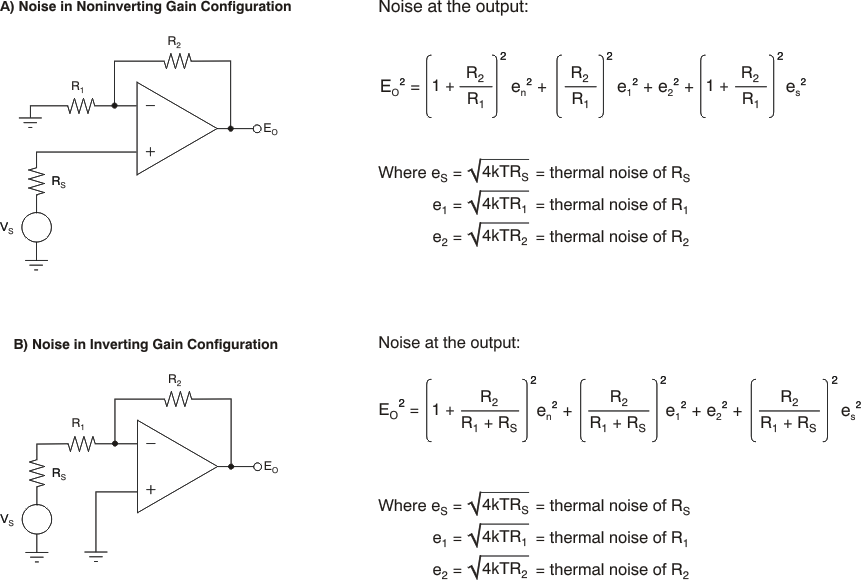
Figure 7-2 illustrates both noninverting (A) and inverting (B) op amp circuit configurations with gain. In circuit configurations with gain, the feedback network resistors also contribute noise. In general, the current noise of the op amp reacts with the feedback resistors to create additional noise components. However, the extremely low current noise of the OPAx140 means that the current noise contribution can be neglected.

The feedback resistor values can generally be chosen to make these noise sources negligible. Low impedance feedback resistors load the output of the amplifier. The equations for total noise are shown for both configurations.
GUID-16CB486C-4E5C-4F85-BA96-86937A81AFDA-low.gif
For the OPAx140 series of operational amplifiers at 1 kHz, en = 5.1 nV/√ Hz.
Figure 7-2 Noise Calculation in Gain Configurations