SBOS727B November 2015 – May 2016 OPA1622
PRODUCTION DATA.
- 1 Features
- 2 Applications
- 3 Description
- 4 Revision History
- 5 Pin Configuration and Functions
- 6 Specifications
- 7 Detailed Description
- 8 Application and Implementation
- 9 Power Supply Recommendations
- 10Layout
- 11Device and Documentation Support
- 12Mechanical, Packaging, and Orderable Information
6 Specifications
6.1 Absolute Maximum Ratings
over operating free-air temperature range (unless otherwise noted)(1)| MIN | MAX | UNIT | |||
|---|---|---|---|---|---|
| Voltage | Supply voltage, VS = (V+) – (V–) | 40 | V | ||
| Input voltage (signal inputs, enable, ground) | (V–) – 0.5 | (V+) + 0.5 | |||
| Input differential voltage | ±0.5 | ||||
| Current | Input current (all pins except power-supply pins) | ±10 | mA | ||
| Output short-circuit(2) | Continuous | ||||
| Temperature | Operating, TA | –55 | 125 | °C | |
| Junction, TJ | 200 | ||||
| Storage, Tstg | –65 | 150 | |||
(1) Stresses beyond those listed under Absolute Maximum Ratings may cause permanent damage to the device. These are stress ratings only, which do not imply functional operation of the device at these or any other conditions beyond those indicated under Recommended Operating Conditions. Exposure to absolute-maximum-rated conditions for extended periods may affect device reliability.
(2) Short-circuit to VS / 2 (ground in symmetrical dual supply setups), one amplifier per package.
6.2 ESD Ratings
| VALUE | UNIT | |||
|---|---|---|---|---|
| V(ESD) | Electrostatic discharge | Human-body model (HBM), per ANSI/ESDA/JEDEC JS-001(1) | ±4000 | V |
| Charged-device model (CDM), per JEDEC specification JESD22-C101(2) | ±1500 | |||
(1) JEDEC document JEP155 states that 500-V HBM allows safe manufacturing with a standard ESD control process.
(2) JEDEC document JEP157 states that 250-V CDM allows safe manufacturing with a standard ESD control process.
6.3 Recommended Operating Conditions
over operating free-air temperature range (unless otherwise noted)| MIN | NOM | MAX | UNIT | ||
|---|---|---|---|---|---|
| Supply voltage, (V+) – (V–) | Single-supply | 4 | 36 | V | |
| Dual-supply | ±2 | ±18 | |||
| Specified temperature | –40 | 125 | °C | ||
6.4 Thermal Information
| THERMAL METRIC(1) | OPA1622 | UNIT | |
|---|---|---|---|
| DRC (SON) | |||
| 10 PINS | |||
| RθJA | Junction-to-ambient thermal resistance | 47.6 | °C/W |
| RθJC(top) | Junction-to-case (top) thermal resistance | 58.1 | °C/W |
| RθJB | Junction-to-board thermal resistance | 22.0 | °C/W |
| ψJT | Junction-to-top characterization parameter | 0.9 | °C/W |
| ψJB | Junction-to-board characterization parameter | 22.2 | °C/W |
| RθJC(bot) | Junction-to-case (bottom) thermal resistance | 4.1 | °C/W |
(1) For more information about traditional and new thermal metrics, see the IC Package Thermal Metrics application report, SPRA953.
6.5 Electrical Characteristics:
at TA = +25°C, VS = ±2 V to ±18 V, VCM = VOUT = midsupply, and RL = 1 kΩ (unless otherwise noted)| PARAMETER | TEST CONDITIONS | MIN | TYP | MAX | UNIT | ||
|---|---|---|---|---|---|---|---|
| AUDIO PERFORMANCE | |||||||
| THD+N | Total harmonic distortion + noise | G = 1, f = 1 kHz, VOUT = 3.5 VRMS, RL = 2 kΩ, 80-kHz measurement bandwidth |
0.000024% | ||||
| –132 | dB | ||||||
| G = 1, f = 1 kHz, VOUT = 3.5 VRMS, RL = 600 Ω, 80-kHz measurement bandwidth |
0.000025% | ||||||
| –132 | dB | ||||||
| G = 1, f = 1 kHz, POUT = 10 mW, RL = 128 Ω, 80-kHz measurement bandwidth |
0.000071% | ||||||
| –123 | dB | ||||||
| G = 1, f = 1 kHz, POUT = 10 mW, RL = 32 Ω, 80-kHz measurement bandwidth |
0.000149% | ||||||
| –116 | dB | ||||||
| G = 1, f = 1 kHz, POUT = 10 mW, RL = 16 Ω, 80-kHz measurement bandwidth |
0.000214% | ||||||
| –113 | dB | ||||||
| IMD | Intermodulation distortion | SMPTE/DIN two-tone, 4:1 (60 Hz and 7 kHz), G = 1, VO = 3 VRMS, RL = 2 kΩ, 90-kHz measurement bandwidth |
0.000018% | ||||
| –135 | dB | ||||||
| CCIF twin-tone (19 kHz and 20 kHz), G = 1, VO = 3 VRMS, RL = 2 kΩ, 90-kHz measurement bandwidth |
0.00005% | ||||||
| –126 | dB | ||||||
| FREQUENCY RESPONSE | |||||||
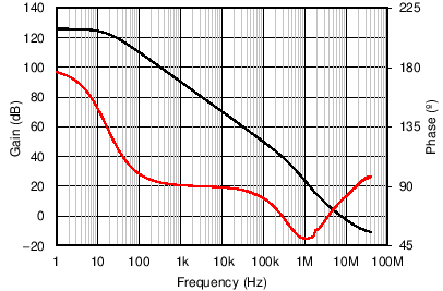
| GBW | Gain-bandwidth product | G = 1000 | 32 | MHz | |||
| G = 1 | 8 | ||||||
| SR | Slew rate | G = –1 | 10 | V/μs | |||
| Full-power bandwidth(1) | VO = 1 VP | 1.6 | MHz | ||||
| Overload recovery time | G = –10 | 300 | ns | ||||
| Channel separation (dual) | f = 1 kHz | 140 | dB | ||||
| NOISE | |||||||
| Input voltage noise | f = 20 Hz to 20 kHz | 2.1 | μVPP | ||||
| en | Input voltage noise density(2) | f = 10 Hz | 10 | nV/√Hz | |||
| f = 100 Hz | 4 | ||||||
| f = 1 kHz | 2.8 | ||||||
| In | Input current noise density | f = 10 Hz | 2.5 | pA/√Hz | |||
| f = 1 kHz | 0.8 | ||||||
| OFFSET VOLTAGE | |||||||
| VOS | Input offset voltage | ±100 | ±500 | μV | |||
| TA = –40°C to +125°C | ±600 | ||||||
| dVOS/dT | Input offset voltage drift(2) | TA = –40°C to +125°C | 0.5 | 2.5 | μV/°C | ||
| PSRR | Power-supply rejection ratio | 0.1 | 3 | μV/V | |||
| INPUT BIAS CURRENT | |||||||
| IB | Input bias current | 1.2 | 2.0 | μA | |||
| TA = –40°C to +125°C(2) | 2.2 | ||||||
| IOS | Input offset current | ±10 | ±50 | nA | |||
| TA = –40°C to +125°C(2) | ±80 | ||||||
| INPUT VOLTAGE RANGE | |||||||
| VCM | Common-mode voltage range | (V–) + 1.5 | (V+) – 1 | V | |||
| CMRR | Common-mode rejection ratio | (V–) + 1.5 V ≤ VCM ≤ (V+) – 1 V, TA = –40°C to +125°C | 110 | 127 | dB | ||
| INPUT IMPEDANCE | |||||||
| Differential | 60k || 0.8 | Ω || pF | |||||
| Common-mode | 500M || 0.9 | Ω || pF | |||||
| OPEN-LOOP GAIN | |||||||
| AOL | Open-loop voltage gain | (V–) + 2 V ≤ VO ≤ (V+) – 2 V, RL = 32 Ω, VS = ± 5 V | 114 | 120 | dB | ||
| (V–) + 1.5 V ≤ VO ≤ (V+) – 1.5 V, RL = 600 Ω, VS = ± 18 V | 120 | 136 | |||||
| OUTPUT | |||||||
| VO | Voltage output swing from rail | Positive rail | No load | 800 | mV | ||
| RL = 600 Ω | 900 | ||||||
| Negative rail | No load | 800 | |||||
| RL = 600 Ω | 900 | ||||||
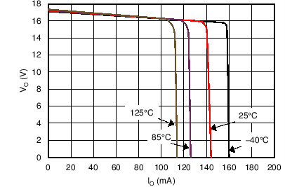
| IOUT | Output current | See Figure 38 and Figure 39 | mA | ||||
| ZO | Open-loop output impedance | See Figure 40 | Ω | ||||
| ISC | Short-circuit current | VS = ±18 V | +145 / –130 | mA | |||
| CLOAD | Capacitive load drive | See Figure 24 | pF | ||||
| ENABLE PIN | |||||||
| VIH | Logic high threshold | 0.82 | V | ||||
| TA = –40°C to +125°C | 0.95 | ||||||
| VIL | Logic low threshold | 0.78 | V | ||||
| TA = –40°C to +125°C | 0.65 | ||||||
| IIH | Input current | VEN = 1.8 V | 1.5 | μA | |||
| POWER SUPPLY | |||||||
| IQ | Quiescent current (per channel) |
VEN = 2.0 V, IOUT = 0 A | 2.6 | 3.3 | mA | ||
| TA = –40°C to +125°C(2) | 4.2 | ||||||
| VEN = 0 V, IOUT = 0 A | 5 | 10 | μA | ||||
(1) Full-power bandwidth = SR / (2π × VP), where SR = slew rate.
(2) Specified by design and characterization.
6.6 Typical Characteristics
at TA = 25°C, VS = ±18 V, and RL = 2 kΩ (unless otherwise noted)
| 9250 channels |

| 4 typical units |


| 600-Ω load |


| 10 mW, 80-kHz measurement bandwidth |

| 1 kHz, 80-kHz measurement bandwidth |


| G = 1, 10 mV |

| G = –10 |


| VS = ±2 V |


| 50 channels |


| 2-kΩ load |

| 3.5 VRMS, 80-kHz measurement bandwidth |

| 1 kHz, 80-kHz measurement bandwidth |

| 90-kHz measurement bandwidth |


| G = 1, 10 V |

| G = –10 |


| VS = ±18 V |


