JAJSD80A June   2017  – November 2017 OPA1641-Q1 , OPA1642-Q1

PRODUCTION DATA.  

  1. 特長
  2. アプリケーション
  3. 概要
  4. 改訂履歴
  5. Pin Configuration and Functions
  6. Specifications
    1. 6.1 Absolute Maximum Ratings
    2. 6.2 ESD Ratings
    3. 6.3 Recommended Operating Conditions
    4. 6.4 Thermal Information
    5. 6.5 Electrical Characteristics
    6. 6.6 Typical Characteristics
  7. Detailed Description
    1. 7.1 Overview
    2. 7.2 Functional Block Diagram
    3. 7.3 Feature Description
      1. 7.3.1 Phase Reversal Protection
      2. 7.3.2 Output Current Limit
      3. 7.3.3 EMI Rejection Ratio (EMIRR)
        1. 7.3.3.1 EMIRR IN+ Test Configuration
    4. 7.4 Device Functional Modes
      1. 7.4.1 Operating Voltage
  8. Application and Implementation
    1. 8.1 Application Information
      1. 8.1.1 Total Harmonic Distortion Measurements
      2. 8.1.2 Source Impedance and Distortion
      3. 8.1.3 Capacitive Load and Stability
      4. 8.1.4 Power Dissipation and Thermal Protection
      5. 8.1.5 Electrical Overstress
    2. 8.2 Typical Application
      1. 8.2.1 Single-Supply Electret Microphone Preamplifier for Speech
        1. 8.2.1.1 Design Requirements
        2. 8.2.1.2 Detailed Design Procedure
        3. 8.2.1.3 Application Curve
  9. Power Supply Recommendations
  10. 10Layout
    1. 10.1 Layout Guidelines
    2. 10.2 Layout Example
  11. 11デバイスおよびドキュメントのサポート
    1. 11.1 デバイス・サポート
      1. 11.1.1 開発サポート
        1. 11.1.1.1 TINA-TI(無料のダウンロード・ソフトウェア)
        2. 11.1.1.2 TI Precision Designs
        3. 11.1.1.3 WEBENCH® Filter Designer
    2. 11.2 ドキュメントのサポート
      1. 11.2.1 関連資料
    3. 11.3 関連リンク
    4. 11.4 ドキュメントの更新通知を受け取る方法
    5. 11.5 コミュニティ・リソース
    6. 11.6 商標
    7. 11.7 静電気放電に関する注意事項
    8. 11.8 Glossary
  12. 12メカニカル、パッケージ、および注文情報

パッケージ・オプション

メカニカル・データ(パッケージ|ピン)
サーマルパッド・メカニカル・データ
発注情報

Pin Configuration and Functions

OPA1641-Q1: D and DGK Packages
8-Pin SOIC and VSSOP
Top View
OPA1641-Q1 OPA1642-Q1 po_so_msop_bos451.gif
NC - no internal connection

Pin Functions: OPA1641-Q1

PIN I/O DESCRIPTION
NAME NO.
–IN 2 I Inverting input
+IN 3 I Noninverting input
NC 1, 5, 8 No connection
OUT 6 O Output
V– 4 Negative (lowest) power supply
V+ 7 Positive (highest) power supply
OPA1642-Q1: D and DGK Packages
8-Pin SOIC and VSSOP
Top View
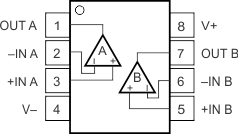
OPA1641-Q1 OPA1642-Q1 po_so_power_bos451.gif

Pin Functions: OPA1642-Q1

PIN I/O DESCRIPTION
NAME NO.
–IN A 2 I Inverting input, channel A
–IN B 6 I Inverting input, channel B
+IN A 3 I Noninverting input, channel A
+IN B 5 I Noninverting input, channel B
OUT A 1 O Output, channel A
OUT B 7 O Output, channel B
V– 4 Negative (lowest) power supply
V+ 8 Positive (highest) power supply