SLOS805C July 2012 – August 2016 OPA1662-Q1
PRODUCTION DATA.
- 1 Features
- 2 Applications
- 3 Description
- 4 Revision History
- 5 Description Continued
- 6 Pin Configuration and Functions
- 7 Specifications
- 8 Detailed Description
- 9 Application and Implementation
- 10Power Supply Recommendations
- 11Layout
- 12Device and Documentation Support
- 13Mechanical, Packaging, and Orderable Information
パッケージ・オプション
メカニカル・データ(パッケージ|ピン)
サーマルパッド・メカニカル・データ
発注情報
7 Specifications
7.1 Absolute Maximum Ratings
over operating free-air temperature range (unless otherwise noted)(1)| MIN | MAX | UNIT | |
|---|---|---|---|
| Supply voltage, (V+) – (V–) | 40 | V | |
| Input voltage | (V–) – 0.5 | (V+) + 0.5 | V |
| Input current (all pins except power-supply pins) | ±10 | mA | |
| Output short-circuit(2) | Continuous | ||
| Operating ambient temperature | –40 | 125 | °C |
| Junction temperature, TJ | 200 | °C | |
| Storage temperature, Tstg | –65 | 150 | °C |
(1) Stresses beyond those listed under Absolute Maximum Ratings may cause permanent damage to the device. These are stress ratings only, which do not imply functional operation of the device at these or any other conditions beyond those indicated under Recommended Operating Conditions. Exposure to absolute-maximum-rated conditions for extended periods may affect device reliability.
(2) Short-circuit to VS / 2 (ground in symmetrical dual supply setups), one amplifier per package.
7.2 ESD Ratings
| VALUE | UNIT | |||
|---|---|---|---|---|
| V(ESD) | Electrostatic discharge | Human-body model (HBM), per AEC Q100-002(1) | ±2000 | V |
| Charged-device model (CDM), per AEC Q100-011 | ±750 | |||
(1) AEC Q100-002 indicates that HBM stressing shall be in accordance with the ANSI/ESDA/JEDEC JS-001 specification.
7.3 Recommended Operating Conditions
over operating free-air temperature range (unless otherwise noted)| MIN | MAX | UNIT | ||
|---|---|---|---|---|
| VS | Supply voltage, (V+) – (V–) | 3 (±1.5) | 36 (±18) | V |
| TA | Operating ambient temperature | –40 | 125 | °C |
7.4 Thermal Information
| THERMAL METRIC(1) | OPA1662-Q1 | UNIT | ||
|---|---|---|---|---|
| D (SOIC) | DGK (VSSOP) | |||
| 8 PINS | 8 PINS | |||
| RθJA | Junction-to-ambient thermal resistance | 156.3 | 225.4 | °C/W |
| RθJC(top) | Junction-to-case (top) thermal resistance | 85.5 | 78.8 | °C/W |
| RθJB | Junction-to-board thermal resistance | 64.9 | 110.5 | °C/W |
| ψJT | Junction-to-top characterization parameter | 33.8 | 14.6 | °C/W |
| ψJB | Junction-to-board characterization parameter | 64.3 | 108.5 | °C/W |
(1) For more information about traditional and new thermal metrics, see the Semiconductor and IC Package Thermal Metrics application report.
7.5 Electrical Characteristics: VS = ±15 V
TA = 25°C, VCM = VOUT = midsupply, and RL = 2 kΩ (unless otherwise noted)| PARAMETER | TEST CONDITIONS | MIN | TYP | MAX | UNIT | ||
|---|---|---|---|---|---|---|---|
| AUDIO PERFORMANCE | |||||||
| THD+N | Total harmonic distortion + noise | G = 1, f = 1 kHz, VO = 3 VRMS | 0.00006% | ||||
| –124 | dB | ||||||
| IMD | Intermodulation distortion | G = 1, VO = 3 VRMS | SMPTE two-tone, 4:1 (60 Hz and 7 kHz) | 0.00004% | |||
| –128 | dB | ||||||
| DIM 30 (3-kHz square wave and 15-kHz sine wave) | 0.00004% | ||||||
| –128 | dB | ||||||
| CCIF twin-tone (19 kHz and 20 kHz) | 0.00004% | ||||||
| –128 | dB | ||||||
| FREQUENCY RESPONSE | |||||||
| GBW | Gain-bandwidth product | G = 1 | 22 | MHz | |||
| SR | Slew rate | G = –1 | 17 | V/µs | |||
| Full power bandwidth(1) | VO = 1 VP | 2.7 | MHz | ||||
| Overload recovery time | G = –10 | 1 | µs | ||||
| Channel separation (dual and quad) | f = 1 kHz | –120 | dB | ||||
| NOISE | |||||||
| en | Input voltage noise | f = 20 Hz to 20 kHz | 2.8 | µVPP | |||
| Input voltage noise density | f = 1 kHz | 3.3 | nV/√Hz | ||||
| f = 100 Hz | 5 | nV/√Hz | |||||
| In | Input current noise density | f = 1 kHz | 1 | pA/√Hz | |||
| f = 100 Hz | 2 | pA/√Hz | |||||
| OFFSET VOLTAGE | |||||||
| VOS | Input offset voltage | VS = ±1.5 V to ±18 V | ±0.5 | ±1.5 | mV | ||
| VS = ±1.5 V to ±18 V, TA = –40°C to 85°(2) | 2 | 8 | µV/°C | ||||
| PSRR | Power-supply rejection ratio | VS = ±1.5 V to ±18 V | 1 | 3 | µV/V | ||
| INPUT BIAS CURRENT | |||||||
| IB | Input bias current | VCM = 0 V | 600 | 1200 | nA | ||
| IOS | Input offset current | VCM = 0 V | ±25 | ±100 | nA | ||
| INPUT VOLTAGE | |||||||
| VCM | Common-mode voltage | (V–) + 0.5 | (V+) – 1 | V | |||
| CMRR | Common-mode rejection ratio | 106 | 114 | dB | |||
| INPUT IMPEDANCE | |||||||
| Differential resistance | 170 | kΩ | |||||
| Differential capacitance | 2 | pF | |||||
| Common-mode resistance | 600 | kΩ | |||||
| Common-mode capacitance | 2.5 | pF | |||||
| OPEN-LOOP GAIN | |||||||
| AOL | Open-loop voltage gain | (V–) + 0.6 V ≤ VO ≤ (V+) – 0.6 V, RL = 2 kΩ | 106 | 114 | dB | ||
| OUTPUT | |||||||
| VOUT | Output voltage | RL = 2 kΩ | (V–) + 0.6 | (V+) – 0.6 | V | ||
| IOUT | Output current | See Typical Characteristics | mA | ||||
| ZO | Open-loop output impedance | See Typical Characteristics | Ω | ||||
| ISC | Short-circuit current(3) | ±50 | mA | ||||
| CLOAD | Capacitive load drive | 200 | pF | ||||
| POWER SUPPLY | |||||||
| VS | Specified voltage | ±1.5 | ±18 | V | |||
| IQ | Quiescent current (per channel) |
IOUT = 0 A | 1.5 | 1.8 | mA | ||
| IOUT = 0 A, TA = –40°C to 85°(2) | 2 | mA | |||||
| TEMPERATURE | |||||||
| Specified temperature | –40 | 85 | °C | ||||
(1) Full-power bandwidth = SR / (2π × VP), where SR = slew rate.
(2) Specified by design and characterization.
(3) One channel at a time.
7.6 Electrical Characteristics: VS = 5 V
TA = 25°C, VCM = VOUT = midsupply, and RL = 2 kΩ (unless otherwise noted)| PARAMETERTEST | CONDITIONS | MIN | TYP | MAX | UNIT | ||
|---|---|---|---|---|---|---|---|
| AUDIO PERFORMANCE | |||||||
| THD+N | Total harmonic distortion + noise | G = 1, f = 1 kHz, VO = 3 VRMS | 0.0001% | ||||
| –120 | dB | ||||||
| IMD | Intermodulation distortion | G = 1, VO = 3 VRMS | SMPTE two-tone, 4:1 (60 Hz and 7 kHz) | 0.00004% | |||
| –128 | dB | ||||||
| DIM 30 (3-kHz square wave and 15-kHz sine wave) | 0.00004% | ||||||
| –128 | dB | ||||||
| CCIF twin-tone (19 kHz and 20 kHz) | 0.00004% | ||||||
| –128 | dB | ||||||
| FREQUENCY RESPONSE | |||||||
| GBW | Gain-bandwidth product | G = 1 | 20 | MHz | |||
| SR | Slew rate | G = –1 | 13 | V/µs | |||
| Full power bandwidth(1) | VO = 1 VP | 2 | MHz | ||||
| Overload recovery time | G = –10 | 1 | µs | ||||
| Channel separation (dual and quad) | f = 1 kHz | –120 | dB | ||||
| NOISE | |||||||
| en | Input voltage noise | f = 20 Hz to 20 kHz | 3.3 | µVPP | |||
| Input voltage noise density | f = 1 kHz | 3.3 | nV/√Hz | ||||
| f = 100 Hz | 5 | nV/√Hz | |||||
| In | Input current noise density | f = 1 kHz | 1 | pA/√Hz | |||
| f = 100 Hz | 2 | pA/√Hz | |||||
| OFFSET VOLTAGE | |||||||
| VOS | Input offset voltage | VS = ±1.5 V to ±18 V | ±0.5 | ±1.5 | mV | ||
| VS = ±1.5 V to ±18 V, TA = –40°C to 85°(2) | 2 | 8 | µV/°C | ||||
| PSRR | Power-supply rejection ratio | VS = ±1.5 V to ±18 V | 1 | 3 | µV/V | ||
| INPUT BIAS CURRENT | |||||||
| IB | Input bias current | VCM = 0 V | 600 | 1200 | nA | ||
| IOS | Input offset current | VCM = 0 V | ±25 | ±100 | nA | ||
| INPUT VOLTAGE | |||||||
| VCM | Common-mode voltage | (V–) + 0.5 | (V+) – 1 | V | |||
| CMRR | Common-mode rejection ratio | 86 | 100 | dB | |||
| INPUT IMPEDANCE | |||||||
| Differential resistance | 170 | kΩ | |||||
| Differential capacitance | 2 | pF | |||||
| Common-mode resistance | 600 | kΩ | |||||
| Common-mode capacitance | 2.5 | pF | |||||
| OPEN-LOOP GAIN | |||||||
| AOL | Open-loop voltage gain | (V–) + 0.6 V ≤ VO ≤ (V+) – 0.6 V, RL = 2 kΩ | 90 | 100 | dB | ||
| OUTPUT | |||||||
| VOUT | Output voltage | RL = 2 kΩ | (V–) + 0.6 | (V+) – 0.6 | V | ||
| IOUT | Output current | See \ | mA | ||||
| ZO | Open-loop output impedance | See Typical Characteristics | Ω | ||||
| ISC | Short-circuit current(3) | ±40 | mA | ||||
| CLOAD | Capacitive load drive | 200 | pF | ||||
| POWER SUPPLY | |||||||
| VS | Specified voltage | ±1.5 | ±18 | V | |||
| IQ | Quiescent current (per channel) | IOUT = 0 A | 1.4 | 1.7 | mA | ||
| IOUT = 0 A, TA = –40°C to 85°(2) | 2 | mA | |||||
| TEMPERATURE | |||||||
| Specified temperature | –40 | 85 | °C | ||||
(1) Full-power bandwidth = SR / (2π × VP), where SR = slew rate.
(2) Specified by design and characterization.
(3) One channel at a time.
7.7 Typical Characteristics
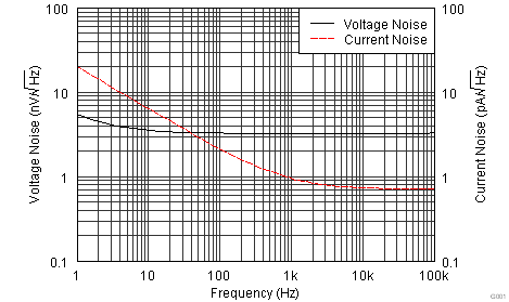
At TA = 25°C, VS = ±15 V, and RL = 2 kΩ (unless otherwise noted) Figure 1. Input Voltage Noise Density and Input Current Noise Density vs Frequency
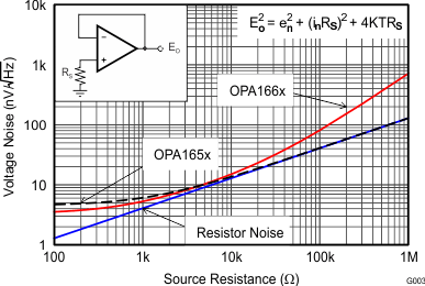
 Figure 3. Voltage Noise vs Source Resistance
 Figure 5. Gain and Phase vs Frequency
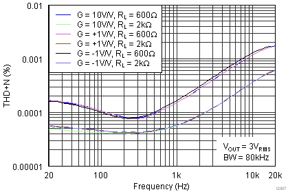
 Figure 7. THD+N Ratio vs Frequency
 Figure 9. THD+N Ratio vs Frequency
 Figure 11. THD+N Ratio vs Frequency
 Figure 13. THD+N Ratio vs Output Amplitude
 Figure 15. Channel Separation vs Frequency
 Figure 17. Small-Signal Step Response
 Figure 19. Small-Signal Step Response
 Figure 21. Large-Signal Step Response
 Figure 23. Large-Signal Step Response
 Figure 25. Small-Signal Overshoot vs Capacitive Load
 Figure 27. Small-Signal Overshoot vs Capacitive Load
 Figure 29. Small-Signal Overshoot vs Feedback Capacitor
 Figure 31. Phase Margin vs Capacitive Load
 Figure 33. IB and IOS vs Temperature
 Figure 35. Supply Current vs Temperature
 Figure 37. Short-Circuit Current vs Temperature
 Figure 39. Positive Overload Recovery
 Figure 41. Open-Loop Output Impedance vs Frequency
 Figure 2. 0.1-Hz to 10-Hz Noise
 Figure 4. Maximum Output Voltage vs Frequency
 Figure 6. Closed-Loop Gain vs Frequency
 Figure 8. THD+N Ratio vs Frequency
 Figure 10. THD+N Ratio vs Frequency
 Figure 12. THD+N Ratio vs Frequency
 Figure 14. Intermodulation Distortion vs Output Amplitude
 Figure 16. CMRR and PSRR vs Frequency
(Referred to Input)
 Figure 18. Small-Signal Step Response
 Figure 20. Small-Signal Step Response
 Figure 22. Large-Signal Step Response
 Figure 24. Large-Signal Step Response
 Figure 26. Small-Signal Overshoot vs Capacitive Load
 Figure 28. Small-Signal Overshoot vs Capacitive Load
 Figure 30. Percent Overshoot vs Capacitive Load
 Figure 32. Open-Loop Gain vs Temperature
 Figure 34. IB and IOS vs Common-Mode Voltage
 Figure 36. Supply Current vs Supply Voltage
 Figure 38. Output Voltage vs Output Current
 Figure 40. Negative Overload Recovery
 Figure 42. No Phase Reversal