SBOS489A December 2011 – December 2024 OPA1662 , OPA1664
PRODUCTION DATA
- 1
- 1Features
- 2Applications
- 3Description
- 4Pin Configurations
- 5Specifications
- 6Application and Implementation
- 7Device and Documentation Support
- 8Revision History
- 9Mechanical, Packaging, and Orderable Information
パッケージ・オプション
デバイスごとのパッケージ図は、PDF版データシートをご参照ください。
メカニカル・データ(パッケージ|ピン)
- D|8
- DGK|8
サーマルパッド・メカニカル・データ
発注情報
6.1.4 Basic Noise Calculations
Design of low-noise op amp circuits requires careful consideration of a variety of possible noise contributors: noise from the signal source, noise generated in the op amp, and noise from the feedback network resistors. The total noise of the circuit is the root-sum-square combination of all noise components.
The resistive portion of the source impedance produces thermal noise proportional to the square root of the resistance. Figure 6-3 plots this equation. The source impedance is usually fixed; consequently, select the op amp and the feedback resistors to minimize the respective contributions to the total noise.
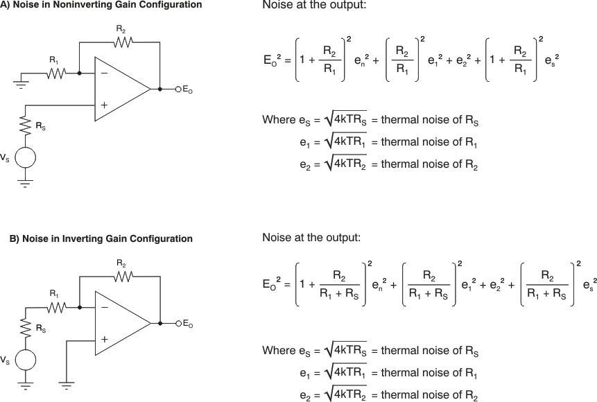
Figure 6-4 illustrates both inverting and noninverting op amp circuit configurations with gain. In circuit configurations with gain, the feedback network resistors also contribute noise. The current noise of the op amp reacts with the feedback resistors to create additional noise components. The feedback resistor values can generally be chosen to make these noise sources negligible. The equations for total noise are shown for both configurations.
