JAJSD62C March 2013 – January 2020 OPA188
PRODUCTION DATA.
- 1 特長
- 2 アプリケーション
- 3 概要
- 4 改訂履歴
- 5 Device Comparison Table
- 6 Pin Configuration and Functions
- 7 Specifications
- 8 Detailed Description
- 9 Application and Implementation
- 10Power Supply Recommendations
- 11Layout
- 12デバイスおよびドキュメントのサポート
- 13メカニカル、パッケージ、および注文情報
パッケージ・オプション
メカニカル・データ(パッケージ|ピン)
サーマルパッド・メカニカル・データ
発注情報
8.3.5 EMI Rejection
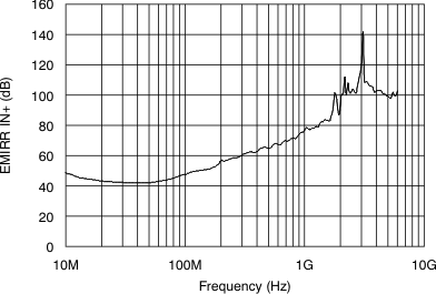
The OPA188 uses integrated electromagnetic interference (EMI) filtering to reduce the effects of EMI interference from sources such as wireless communications and densely-populated boards with a mix of analog signal chain and digital components. EMI immunity can be improved with circuit design techniques; the benefits from these design improvements. Texas Instruments™ has developed the ability to accurately measure and quantify the immunity of an operational amplifier over a broad frequency spectrum extending from 10 MHz to 6 GHz. Figure 40 shows the results of this testing on the OPA188 . Table 4 lists the EMIRR IN+ values for theOPA188 at particular frequencies commonly encountered in real-world applications. Applications listed in Table 4 may be centered on or operated near the particular frequency shown. Detailed information can also be found in EMI Rejection Ratio of Operational Amplifiers, available for download from www.ti.com.
 Figure 40. EMIRR Testing
 Table 4. OPA188 EMIRR IN+ for Frequencies of Interest
| FREQUENCY | APPLICATION OR ALLOCATION | EMIRR IN+ |
|---|---|---|
| 400 MHz | Mobile radio, mobile satellite, space operation, weather, radar, ultra-high frequency (UHF) applications | 62.2 dB |
| 900 MHz | Global system for mobile communications (GSM) applications, radio communication, navigation, GPS (to 1.6 GHz), GSM, aeronautical mobile, UHF applications | 74.7 dB |
| 1.8 GHz | GSM applications, mobile personal communications, broadband, satellite, L-band (1 GHz to 2 GHz) | 100.7 dB |
| 2.4 GHz | 802.11b, 802.11g, 802.11n, Bluetooth®, mobile personal communications, industrial, scientific and medical (ISM) radio band, amateur radio and satellite, S-band (2 GHz to 4 GHz) | 102.4 dB |
| 3.6 GHz | Radiolocation, aero communication and navigation, satellite, mobile, S-band | 104.8 dB |
| 5 GHz | 802.11a, 802.11n, aero communication and navigation, mobile communication, space and satellite operation, C-band (4 GHz to 8 GHz) | 100.3 dB |