JAJSG31B September 2018 – June 2019 OPA2156
PRODUCTION DATA.
- 1 特長
- 2 アプリケーション
- 3 概要
- 4 改訂履歴
- 5 概要(続き)
- 6 Pin Configuration and Functions
- 7 Specifications
- 8 Detailed Description
- 9 Application and Implementation
- 10Power Supply Recommendations
- 11Layout
- 12デバイスおよびドキュメントのサポート
- 13メカニカル、パッケージ、および注文情報
パッケージ・オプション
メカニカル・データ(パッケージ|ピン)
サーマルパッド・メカニカル・データ
発注情報
8.3.3 Thermal Considerations
Through normal operation the OPA2156 will experience self-heating, a natural increase in the die junction temperature which occurs in every amplifier. This is a result of several factors including the quiescent power consumption, the package’s thermal dissipation, PCB layout and the device operating conditions.
To fully ensure the amplifier will operate without entering thermal shutdown it is important to calculate the approximate junction (die) temperature which can be done using Equation 1.

Equation 2 shows the approximate junction temperature for the OPA2156 while unloaded with an ambient temperature of 25°C.

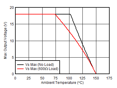
For high voltage, high precision amplifiers such as the OPA2156 the junction temperature can easily be 10s of degrees higher than the ambient temperature in a quiescent (unloaded) condition. If the device then begins to drive a heavy load the junction temperature may rise and trip the thermal shutdown circuit. The Figure 44 shows the maximum output voltage of the OPA2156 without entering thermal shutdown vs ambient temperature in both a loaded and unloaded condition.
 Figure 44. OPA2156 Thermal Safe Operating Area