JAJSD63A June   2017  – June 2018 OPA180-Q1 , OPA2180-Q1

PRODUCTION DATA.  

  1. 特長
  2. アプリケーション
  3. 概要
    1.     低ノイズ (ピーク・ツー・ピークのノイズ = 250nV)
  4. 改訂履歴
  5. Device Comparison Table
  6. Pin Configuration and Functions
    1.     Pin Functions: OPA180-Q1
    2.     Pin Functions: OPA2180-Q1
  7. Specifications
    1. 7.1 Absolute Maximum Ratings
    2. 7.2 ESD Ratings
    3. 7.3 Recommended Operating Conditions
    4. 7.4 Thermal Information: OPA180-Q1
    5. 7.5 Thermal Information: OPA2180-Q1
    6. 7.6 Electrical Characteristics: VS = ±2 V to ±18 V (VS = 4 V to 36 V)
    7. 7.7 Typical Characteristics: Table of Graphs
    8. 7.8 Typical Characteristics
  8. Detailed Description
    1. 8.1 Overview
    2. 8.2 Functional Block Diagram
    3. 8.3 Feature Description
      1. 8.3.1 Operating Characteristics
      2. 8.3.2 EMI Rejection
      3. 8.3.3 Phase-Reversal Protection
      4. 8.3.4 Capacitive Load and Stability
      5. 8.3.5 Electrical Overstress
    4. 8.4 Device Functional Modes
  9. Application and Implementation
    1. 9.1 Application Information
    2. 9.2 Typical Applications
      1. 9.2.1 Bipolar ±10-V Analog Output from a Unipolar Voltage Output DAC
        1. 9.2.1.1 Design Requirements
        2. 9.2.1.2 Detailed Design Procedure
          1. 9.2.1.2.1 Component Selection
        3. 9.2.1.3 Application Curves
      2. 9.2.2 Discrete INA + Attenuation
      3. 9.2.3 RTD Amplifier
  10. 10Power Supply Recommendations
  11. 11Layout
    1. 11.1 Layout Guidelines
    2. 11.2 Layout Example
  12. 12デバイスおよびドキュメントのサポート
    1. 12.1 関連リンク
    2. 12.2 商標
    3. 12.3 静電気放電に関する注意事項
    4. 12.4 Glossary
  13. 13メカニカル、パッケージ、および注文情報

パッケージ・オプション

メカニカル・データ(パッケージ|ピン)
サーマルパッド・メカニカル・データ
発注情報

Typical Characteristics

VS = ±18 V, VCM = VS / 2, RLOAD = 10 kΩ connected to VS / 2, and CL = 100 pF, unless otherwise noted.
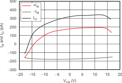
OPA180-Q1 OPA2180-Q1 tc_ib_ios-vcm_bos584.gif
Figure 1. IIB and IIO vs Common-Mode Voltage
OPA180-Q1 OPA2180-Q1 tc_vo_swing-io_bos584.gif
Figure 3. Output Voltage Swing vs Output Current
(Maximum Supply)
OPA180-Q1 OPA2180-Q1 tc_noise_bos584.gif
Peak-to-Peak Noise = 250 nV
Figure 5. 0.1-Hz to 10-Hz Noise
OPA180-Q1 OPA2180-Q1 tc_g_ph-frq_bos525.png
Figure 7. Open-Loop Gain and Phase vs Frequency
OPA180-Q1 OPA2180-Q1 tc_oloop_iout-frq_bos525.gif
Figure 9. Open-Loop Output Impedance vs Frequency
OPA180-Q1 OPA2180-Q1 tc_sm_oshoot-cl_neg_bos584.gif
RL = 10 kΩ
Figure 11. Small-Signal Overshoot vs Capacitive Load
(100-mV Output Step)
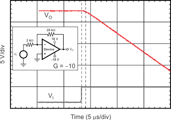
OPA180-Q1 OPA2180-Q1 tc_oload_pos_bos584.gif
Figure 13. Positive Overload Recovery
OPA180-Q1 OPA2180-Q1 tc_sm_step_pos_bos584.gif
RL = 10 kΩ CL = 10 pF
Figure 15. Small-Signal Step Response
(100 mV)
OPA180-Q1 OPA2180-Q1 tc_lg_step_pos_bos584.gif
G = 1 RL = 10 kΩ CL = 10 pF
Figure 17. Large-Signal Step Response
OPA180-Q1 OPA2180-Q1 tc_lg_t_pos_bos584.gif
G = –1
Figure 19. Large-Signal Settling Time (10-V Positive Step)
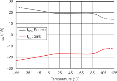
OPA180-Q1 OPA2180-Q1 tc_isc-tmp_bos584.gif
Figure 21. Short-Circuit Current vs Temperature
OPA180-Q1 OPA2180-Q1 tc_ch_sep-frq_bos584.gif
Figure 23. Channel Separation vs Frequency
OPA180-Q1 OPA2180-Q1 tc_ibias-tmp_bos584.gif
Figure 2. Input Bias Current vs Temperature
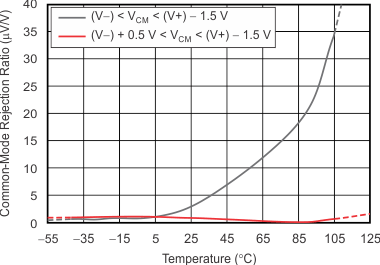
OPA180-Q1 OPA2180-Q1 tc_cmrr-tmp_2v_bos584.gif
VSUPPLY = ±2 V
Figure 4. CMRR vs Temperature
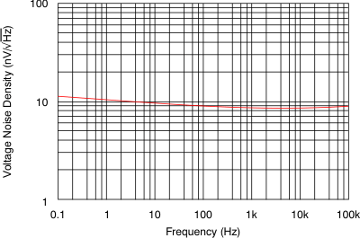
OPA180-Q1 OPA2180-Q1 tc_noise_spec-frq_bos525.gif
Figure 6. Input Voltage Noise Spectral Density vs Frequency
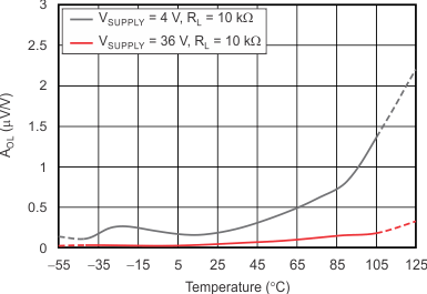
OPA180-Q1 OPA2180-Q1 tc_oloop_g-tmp_bos584.gif
Figure 8. Open-Loop Gain vs Temperature
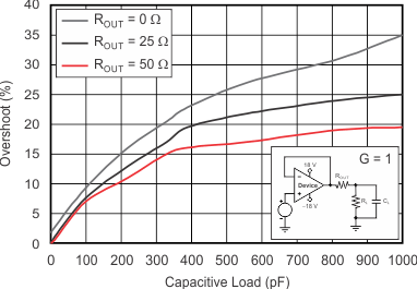
OPA180-Q1 OPA2180-Q1 tc_sm_oshoot-cl_pos_bos584.gif
RL = 10 kΩ
Figure 10. Small-Signal Overshoot vs Capacitive Load
(100-mV Output Step)
OPA180-Q1 OPA2180-Q1 tc_no_phase_bos584.gif
Figure 12. No Phase Reversal
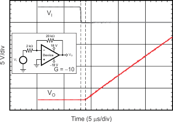
OPA180-Q1 OPA2180-Q1 tc_oload_neg_bos584.gif
Figure 14. Negative Overload Recovery
OPA180-Q1 OPA2180-Q1 tc_sm_step_neg_bos584.gif
RL = 10 kΩ CL = 10 pF
Figure 16. Small-Signal Step Response (100 mV)
OPA180-Q1 OPA2180-Q1 tc_lg_step_neg_bos584.gif
G = –1 RL = 10 kΩ CL = 10 pF
Figure 18. Large-Signal Step Response
OPA180-Q1 OPA2180-Q1 tc_lg_t_neg_bos584.gif
G = –1
Figure 20. Large-Signal Settling Time (10-V Negative Step)
OPA180-Q1 OPA2180-Q1 tc_max_vo-frq_bos525.gif
Figure 22. Maximum Output Voltage vs Frequency
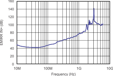
OPA180-Q1 OPA2180-Q1 tc_emirr-frq_bos584.gif
Figure 24. EMIRR IN+ vs Frequency