JAJSD63A June   2017  – June 2018 OPA180-Q1 , OPA2180-Q1

PRODUCTION DATA.  
  1. 特長
  2. アプリケーション
  3. 概要
    1.     低ノイズ (ピーク・ツー・ピークのノイズ = 250nV)
  4. 改訂履歴
  5. Device Comparison Table
  6. Pin Configuration and Functions
    1.     Pin Functions: OPA180-Q1
    2.     Pin Functions: OPA2180-Q1
  7. Specifications
    1. 7.1 Absolute Maximum Ratings
    2. 7.2 ESD Ratings
    3. 7.3 Recommended Operating Conditions
    4. 7.4 Thermal Information: OPA180-Q1
    5. 7.5 Thermal Information: OPA2180-Q1
    6. 7.6 Electrical Characteristics: VS = ±2 V to ±18 V (VS = 4 V to 36 V)
    7. 7.7 Typical Characteristics: Table of Graphs
    8. 7.8 Typical Characteristics
  8. Detailed Description
    1. 8.1 Overview
    2. 8.2 Functional Block Diagram
    3. 8.3 Feature Description
      1. 8.3.1 Operating Characteristics
      2. 8.3.2 EMI Rejection
      3. 8.3.3 Phase-Reversal Protection
      4. 8.3.4 Capacitive Load and Stability
      5. 8.3.5 Electrical Overstress
    4. 8.4 Device Functional Modes
  9. Application and Implementation
    1. 9.1 Application Information
    2. 9.2 Typical Applications
      1. 9.2.1 Bipolar ±10-V Analog Output from a Unipolar Voltage Output DAC
        1. 9.2.1.1 Design Requirements
        2. 9.2.1.2 Detailed Design Procedure
          1. 9.2.1.2.1 Component Selection
        3. 9.2.1.3 Application Curves
      2. 9.2.2 Discrete INA + Attenuation
      3. 9.2.3 RTD Amplifier
  10. 10Power Supply Recommendations
  11. 11Layout
    1. 11.1 Layout Guidelines
    2. 11.2 Layout Example
  12. 12デバイスおよびドキュメントのサポート
    1. 12.1 関連リンク
    2. 12.2 商標
    3. 12.3 静電気放電に関する注意事項
    4. 12.4 Glossary
  13. 13メカニカル、パッケージ、および注文情報

パッケージ・オプション

メカニカル・データ(パッケージ|ピン)
サーマルパッド・メカニカル・データ
発注情報

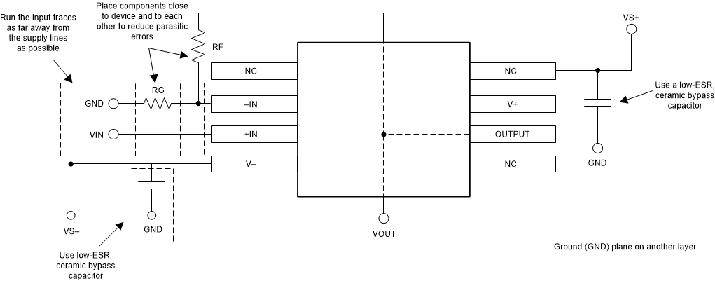
Layout Example

OPA180-Q1 OPA2180-Q1 layout_example_bos620.gifFigure 35. Operational Amplifier Board Layout for Noninverting Configuration