JAJSEY7C January   2016  – March 2018 OPA197 , OPA2197 , OPA4197

PRODUCTION DATA.  

  1. 特長
  2. アプリケーション
  3. 概要
    1.     Device Images
      1.      高電圧の多重化データ収集システムにおけるOPA197
  4. 改訂履歴
  5. Pin Configuration and Functions
    1.     Pin Functions: OPA197
    2.     Pin Functions: OPA2197 and OPA4197
  6. Specifications
    1. 6.1 Absolute Maximum Ratings
    2. 6.2 ESD Ratings
    3. 6.3 Recommended Operating Conditions
    4. 6.4 Thermal Information: OPA197
    5. 6.5 Thermal Information: OPA2197
    6. 6.6 Thermal Information: OPA4197
    7. 6.7 Electrical Characteristics: VS = ±4 V to ±18 V (VS = 8 V to 36 V)
    8. 6.8 Electrical Characteristics: VS = ±2.25 V to ±4 V (VS = 4.5 V to 8 V)
    9. 6.9 Typical Characteristics
  7. Detailed Description
    1. 7.1 Overview
    2. 7.2 Functional Block Diagram
    3. 7.3 Feature Description
      1. 7.3.1 Input Protection Circuitry
      2. 7.3.2 EMI Rejection
      3. 7.3.3 Phase Reversal Protection
      4. 7.3.4 Thermal Protection
      5. 7.3.5 Capacitive Load and Stability
      6. 7.3.6 Common-Mode Voltage Range
      7. 7.3.7 Electrical Overstress
      8. 7.3.8 Overload Recovery
    4. 7.4 Device Functional Modes
  8. Application and Implementation
    1. 8.1 Application Information
    2. 8.2 Typical Applications
      1. 8.2.1 16-Bit Precision Multiplexed Data-Acquisition System
        1. 8.2.1.1 Design Requirements
        2. 8.2.1.2 Detailed Design Procedure
        3. 8.2.1.3 Application Curve
      2. 8.2.2 Slew Rate Limit for Input Protection
      3. 8.2.3 Precision Reference Buffer
  9. Power Supply Recommendations
  10. 10Layout
    1. 10.1 Layout Guidelines
    2. 10.2 Layout Example
  11. 11デバイスおよびドキュメントのサポート
    1. 11.1 デバイス・サポート
      1. 11.1.1 開発サポート
        1. 11.1.1.1 TINA-TI(無料のダウンロード・ソフトウェア)
        2. 11.1.1.2 TI Precision Designs
    2. 11.2 ドキュメントのサポート
      1. 11.2.1 関連資料
    3. 11.3 関連リンク
    4. 11.4 ドキュメントの更新通知を受け取る方法
    5. 11.5 コミュニティ・リソース
    6. 11.6 商標
    7. 11.7 静電気放電に関する注意事項
    8. 11.8 Glossary
  12. 12メカニカル、パッケージ、および注文情報

パッケージ・オプション

メカニカル・データ(パッケージ|ピン)
サーマルパッド・メカニカル・データ
発注情報

Typical Characteristics

Table 1. Table of Graphs

DESCRIPTION FIGURE
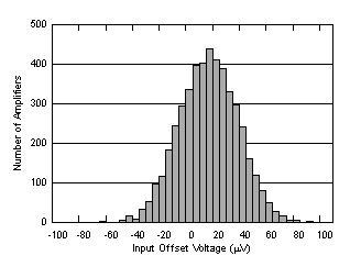
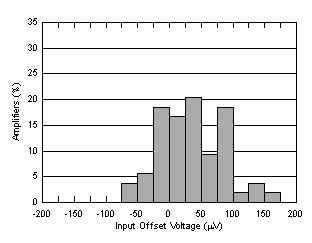
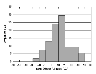
Offset Voltage Production Distribution Figure 1, Figure 2, Figure 3
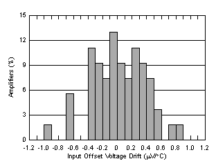
Offset Voltage Drift Distribution Figure 4
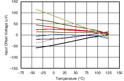
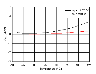
Offset Voltage vs Temperature Figure 5
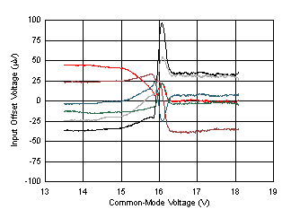
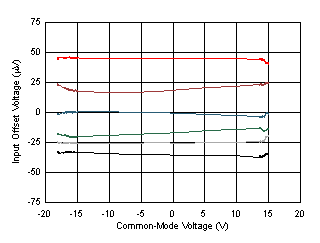
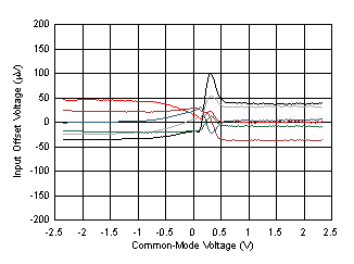
Offset Voltage vs Common-Mode Voltage Figure 6, Figure 7, Figure 8
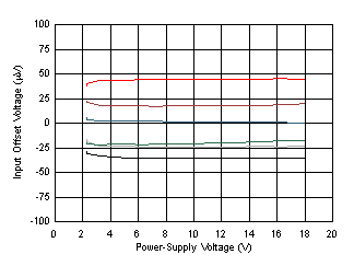
Offset Voltage vs Power Supply Figure 9
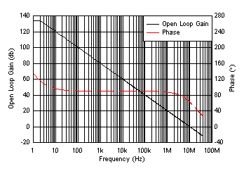
Open-Loop Gain and Phase vs Frequency Figure 10
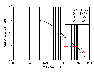
Closed-Loop Gain and Phase vs Frequency Figure 11
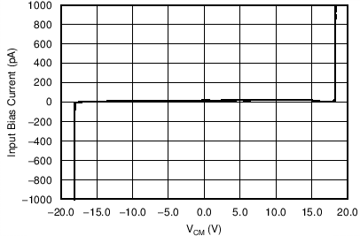
Input Bias Current vs Common-Mode Voltage Figure 12
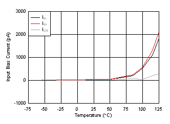
Input Bias Current vs Temperature Figure 13
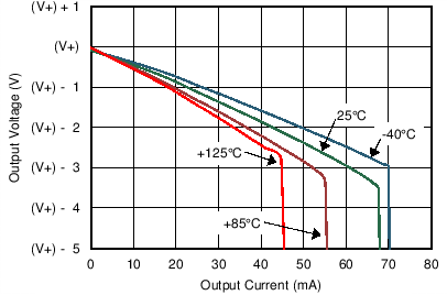
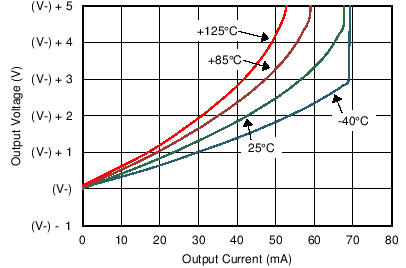
Output Voltage Swing vs Output Current (maximum supply) Figure 14, Figure 15
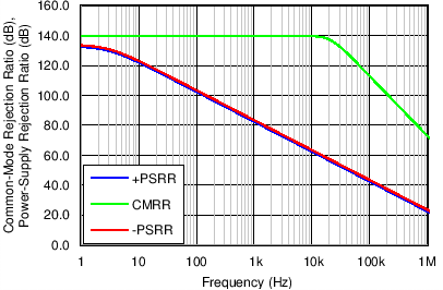
CMRR and PSRR vs Frequency Figure 16
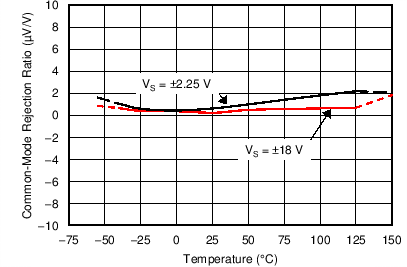
CMRR vs Temperature Figure 17
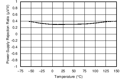
PSRR vs Temperature Figure 18
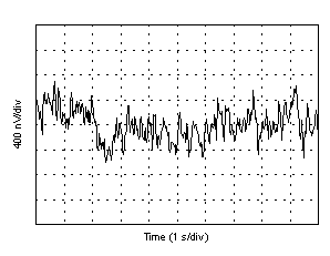
0.1-Hz to 10-Hz Noise Figure 19
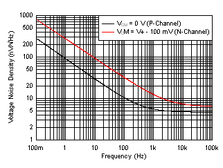
Input Voltage Noise Spectral Density vs Frequency Figure 20
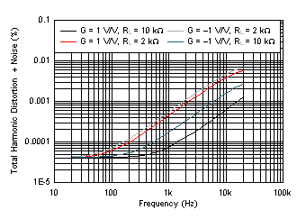
THD+N Ratio vs Frequency Figure 21
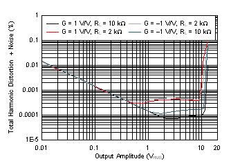
THD+N vs Output Amplitude Figure 22
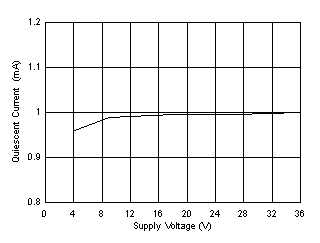
Quiescent Current vs Supply Voltage Figure 23
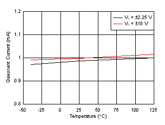
Quiescent Current vs Temperature Figure 24
Open Loop Gain vs Temperature Figure 25
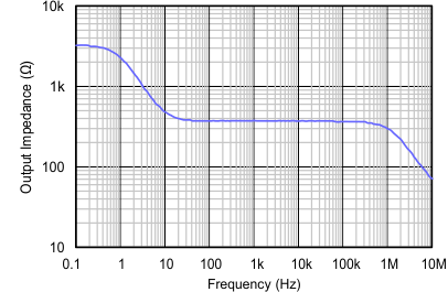
Open Loop Output Impedance vs Frequency Figure 26
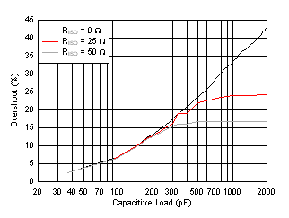
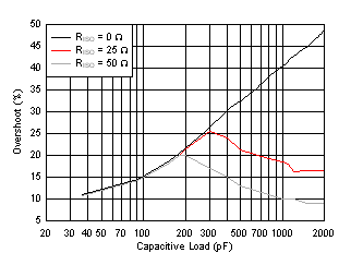
Small Signal Overshoot vs Capacitive Load (100-mV output step) Figure 27, Figure 28
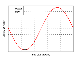
No Phase Reversal Figure 29
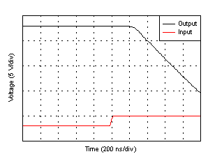
Positive Overload Recovery Figure 30
Negative Overload Recovery Figure 31
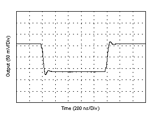
Small-Signal Step Response (100 mV) Figure 32, Figure 33
Large-Signal Step Response Figure 34
Settling Time Figure 35, Figure 36, ,
Short-Circuit Current vs Temperature Figure 37
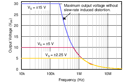
Maximum Output Voltage vs Frequency Figure 38
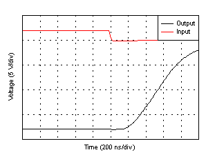
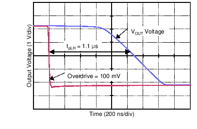
Propagation Delay Rising Edge Figure 39
Propagation Delay Falling Edge Figure 40
at TA = 25°C, VS = ±18 V, VCM = VS / 2, RLOAD = 10 kΩ connected to VS / 2, and CL = 100 pF (unless otherwise noted)
OPA197 OPA2197 OPA4197 D040_SBOS737.gif
4770 production units
Figure 1. Offset Voltage Production Distribution at 25°C
OPA197 OPA2197 OPA4197 D024_SBOS737.gif
Figure 3. Offset Voltage Production Distribution at –40°C
OPA197 OPA2197 OPA4197 C001_OT.png
9 typical units
Figure 5. Offset Voltage vs Temperature
OPA197 OPA2197 OPA4197 D003_SBOS737.gif
6 typical units
Figure 7. Offset Voltage vs Common-Mode Voltage
OPA197 OPA2197 OPA4197 D006_SBOS737.gif
6 typical units
Figure 9. Offset Voltage vs Power Supply
OPA197 OPA2197 OPA4197 D053_SBOS737.gif
Figure 11. Closed-Loop Gain and Phase vs Frequency
OPA197 OPA2197 OPA4197 D015_SBOS737.gif
Figure 13. Input Bias Current vs Temperature
OPA197 OPA2197 OPA4197 C019_OT.png
Figure 15. Output Voltage Swing from Positive Power Supply vs Output Current (Maximum Supply)
OPA197 OPA2197 OPA4197 C008_OT.png
Figure 17. CMRR vs Temperature
OPA197 OPA2197 OPA4197 D001_SBOS737.gif
Peak-to-peak noise = VRMS × 6.6 = 1.30 VPP
Figure 19. 0.1-Hz to 10-Hz Noise
OPA197 OPA2197 OPA4197 D007_SBOS737.gif
VOUT = 3.5 VRMS, BW = 80 kHz
Figure 21. THD+N Ratio vs Frequency
OPA197 OPA2197 OPA4197 C012_OT.gif
Figure 23. Quiescent Current vs Supply Voltage
OPA197 OPA2197 OPA4197 C009_OT.gif
Figure 25. Open-Loop Gain vs Temperature
OPA197 OPA2197 OPA4197 D030_SBOS737.gif
G = –1 V/V
Figure 27. Small-Signal Overshoot vs Capacitive Load
(100-mV Output Step)
OPA197 OPA2197 OPA4197 D032_SBOS737.gif
VS = ±18 V, input = ±18.5 VPP
Figure 29. No Phase Reversal
OPA197 OPA2197 OPA4197 D034_SBOS737.gif
G = –10 V/V
Figure 31. Negative Overload Recovery
OPA197 OPA2197 OPA4197 D036_SBOS737.gif
G = –1 V/V
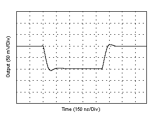
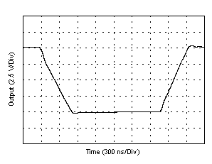
Figure 33. Small-Signal Step Response
OPA197 OPA2197 OPA4197 D134_SBOS737.gif
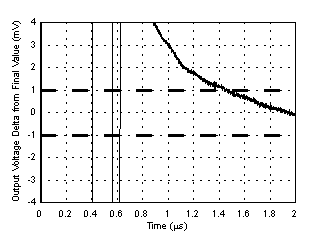
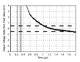
G = 1, 0.01% settling = ±1 mV, step applied at t = 0
Figure 35. Settling Time (10-V Positive Step)
OPA197 OPA2197 OPA4197 D016_SBOS737.gif
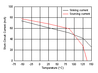
Figure 37. Short-Circuit Current vs Temperature
OPA197 OPA2197 OPA4197 C025_.png
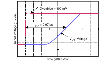
Figure 39. Propagation Delay Rising Edge
OPA197 OPA2197 OPA4197 D028_SBOS737.gif
Figure 2. Offset Voltage Production Distribution at 125°C
OPA197 OPA2197 OPA4197 D021_SBOS737.gif
Figure 4. Offset Voltage Drift Distribution
from –40°C to +125°C
OPA197 OPA2197 OPA4197 D002_SBOS737.gif
6 typical units
Figure 6. Offset Voltage vs Common-Mode Voltage
OPA197 OPA2197 OPA4197 D005_SBOS737.gif
6 typical units
Figure 8. Offset Voltage vs Common-Mode Voltage
OPA197 OPA2197 OPA4197 D004_SBOS737.gif
CLOAD = 15 pF
Figure 10. Open-Loop Gain and Phase vs Frequency
OPA197 OPA2197 OPA4197 C017_OT.png
Figure 12. Input Bias Current vs Common-Mode Voltage
OPA197 OPA2197 OPA4197 C018_OT.png
Figure 14. Output Voltage Swing from Negative Power Supply vs Output Current (Maximum Supply)
OPA197 OPA2197 OPA4197 C012_SBOS620.png
Figure 16. CMRR and PSRR vs Frequency
OPA197 OPA2197 OPA4197 C007_OT.png
Figure 18. PSRR vs Temperature
OPA197 OPA2197 OPA4197 D052_SBOS737.gif
Figure 20. Input Voltage Noise Spectral Density
vs Frequency
OPA197 OPA2197 OPA4197 D008_SBOS737.gif
f = 1 kHz, BW = 80 kHz
Figure 22. THD+N vs Output Amplitude
OPA197 OPA2197 OPA4197 C011_OT.gif
Figure 24. Quiescent Current vs Temperature
OPA197 OPA2197 OPA4197 C016_SBOS737.gif
Figure 26. Open-Loop Output Impedance vs Frequency
OPA197 OPA2197 OPA4197 D031_SBOS737.gif
G = 1 V/V
Figure 28. Small-Signal Overshoot vs Capacitive Load
(100-mV Output Step)
OPA197 OPA2197 OPA4197 D033_SBOS737.gif
G = –10 V/V
Figure 30. Positive Overload Recovery
OPA197 OPA2197 OPA4197 D035_SBOS737.gif
G = 1 V/V
Figure 32. Small-Signal Step Response
OPA197 OPA2197 OPA4197 D037_SBOS737.gif
G = 1 V/V
Figure 34. Large-Signal Step Response
OPA197 OPA2197 OPA4197 D135_SBOS737.gif
G = 1, 0.01% settling = ±500 µV, step applied at t = 0
Figure 36. Settling Time (5-V Positive Step)
OPA197 OPA2197 OPA4197 C033_.png
Figure 38. Maximum Output Voltage vs Frequency
OPA197 OPA2197 OPA4197 C026_.png
Figure 40. Propagation Delay Falling Edge