SLOS896B December 2014 – January 2017 OPA2314-Q1 , OPA314-Q1 , OPA4314-Q1
PRODUCTION DATA.
1 Features
- Qualified for Automotive Applications
- AEC-Q100 Qualified With the Following Results:
- Device Temperature Grade : –40°C to +125°C Ambient Operating Temperature Range
- Device HBM Classification Level 2
- Device CDM Classification Level C6
- Low IQ: 150 µA/ch
- Wide Supply Range: 1.8 V to 5.5 V
- Low Noise: 14 nV/√Hz at 1 kHz
- Gain Bandwidth: 3 MHz
- Low Input Bias Current: 0.2 pA
- Low Offset Voltage: 0.5 mV
- Unity-Gain Stable
- Internal RF and EMI Filter
- Specified Temperature Range:
–40°C to +125°C
2 Applications
- Automotive Applications:
- ADAS
- Body Electronics and Lighting
- Current Sensing
- Battery Monitoring
3 Description
The OPAx314-Q1 series is a family of single–, and dual–, and quad-channel operational amplifiers (op amps) that represents a new generation of low-power, general-purpose CMOS amplifiers. Rail-to-rail input and output swings, low quiescent current (150 μA typically at 5 VS) combined with a wide bandwidth of 3 MHz, and very low noise (14 nV/√Hz at 1 kHz) make this device family very attractive for a variety of battery-powered applications that require a good balance between cost and performance. The low-input bias current supports applications with megaohm source impedances.
The robust design of the OPAx314-Q1 series provides ease-of-use to the circuit designer: unity-gain stability with capacitive loads of up to 300 pF, an integrated RF and EMI rejection filter, no phase reversal in overdrive conditions, and high electrostatic discharge (ESD) protection (4-kV HBM).
The device is optimized for low-voltage operation as low as 1.8 V (±0.9 V) and up to 5.5 V (±2.75 V), and is specified over the full extended temperature range of –40°C to +125°C.
The single-channel device, OPA314-Q1, is offered in the SOT-23 package and the dual-channel device, OPA2314-Q1, is offered in the VSSOP (8) package. The quad-channel OPA4314-Q1 is available in the 14-pin TSSOP package.
Device Information(1)
| PART NUMBER | PACKAGE | BODY SIZE (NOM) |
|---|---|---|
| OPA314-Q1 | SOT-23 (5) | 2.90 mm × 1.60 mm |
| OPA2314-Q1 | VSSOP (8) | 4.90 mm × 3.91 mm |
| OPA4314-Q1 | TSSOP (14) | 5.00 mm × 4.40 mm |
- For all available packages, see the orderable addendum at the end of the data sheet.
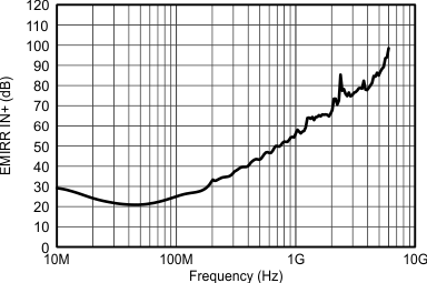
EMIRR vs Frequency

4 Revision History
Changes from A Revision (January 2015) to B Revision
- Added part number OPA4314-Q1 to documentGo
- Added part number OPA4314-Q1 to the Device Information table Go
- Changed OPA2314-Q1 package from SOIC (8) to VSSOP (8) in the Device Information tableGo
- Added OPA314-Q1 (SOT-23 package) throughout documentGo
- Added pinout drawing for the OPA4314-Q1 device in the Pin Configurations and Functions section Go
- Added the Pin Functions: OPA4314-Q1 table to the Pin Configurations and Functions section Go
- Changed formatting of all Thermal Information table notes Go
- Added footnotes to all Thermal Information tablesGo
- Added Thermal Information: OPA4314-Q1 tableGo
- Changed formatting of application report reference in the EMI Susceptibility and Input Filtering section Go
- Changed package drawing to reflect an example of the 5-pin SOT-23 package in the Layout Example sectionGo
- Changed formatting of Related Documentation section Go
- Added part number OPA4314-Q1 to the Related Links table Go
Changes from * Revision (December 2014) to A Revision
- Changed the device status from Product Preview to Production Data Go